Applications information – Rainbow Electronics MAX534 User Manual
Page 13
MAX534
+5V, Low-Power, 8-Bit Quad DAC
with Rail-to-Rail Output Buffers
______________________________________________________________________________________
13
__________Applications Information
DAC Linearity and Voltage Offset
The output buffer can have a negative input offset volt-
age that would normally drive the output negative, but
since there is no negative supply the output stays at 0V
(Figure 9). When linearity is determined using the end-
point method, it is measured between zero code (all
inputs 0) and full-scale code (all inputs 1) after offset
and gain error are calibrated out. However, in single-
supply operation the next code after zero may not
change the output, so the lowest code that produces a
positive output is the lower endpoint.
Power Sequencing
The voltage applied to REF should not exceed V
DD
at
any time. If proper power sequencing is not possible,
connect an external Schottky diode between REF and
V
DD
to ensure compliance with the absolute maximum
ratings. Do not apply signals to the digital inputs before
the device is fully powered up.
Power-Supply Bypassing
and Ground Management
Connect AGND and DGND together at the IC. This
ground should then return to the highest-quality ground
available. Bypass V
DD
with a 0.1µF capacitor, located
as close to V
DD
and DGND as possible.
Careful PC board layout minimizes crosstalk among
DAC outputs and digital inputs. Figure 10 shows sug-
gested circuit board layout to minimize crosstalk.
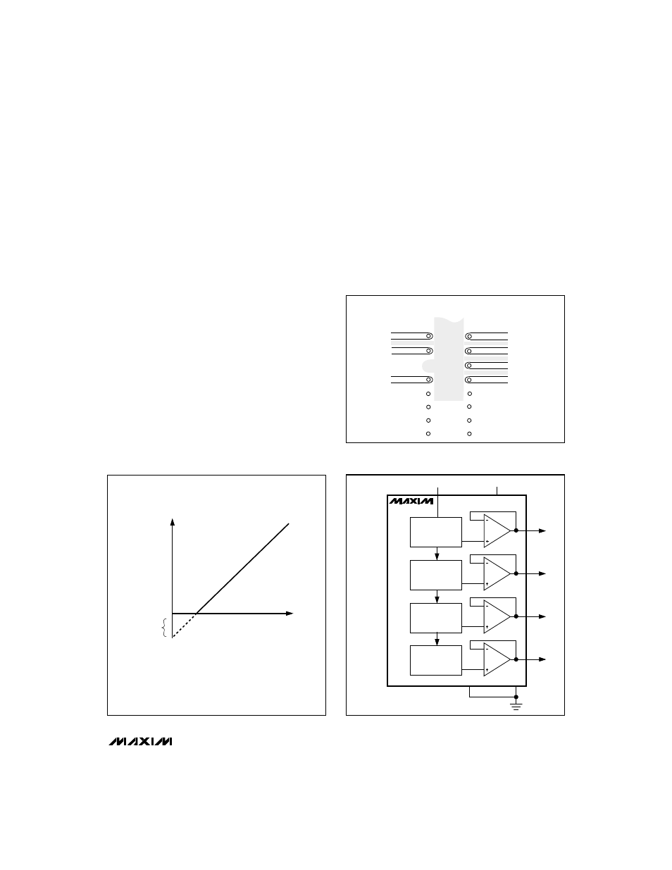
Unipolar-Output,
Two-Quadrant Multiplication
In unipolar operation, the output voltages and the refer-
ence input are the same polarity. Figure 11 shows the
MAX534 unipolar configuration, and Table 2 shows the
unipolar code.
DAC CODE
0V
NEGATIVE
OFFSET
OUTPUT
VOLTAGE
Figure 9. Effect of Negative Offset (Single Supply)
OUTC
OUTD
AGND
OUTB
OUTA
REF
SYSTEM GND
Figure 10. Suggested PC Board Layout for Minimizing
Crosstalk (Bottom View)
DAC A
DAC B
DAC C
DAC D
REFAB
MAX534
OUTA
OUTB
OUTC
OUTD
SERIAL
INTERFACE
NOT SHOWN
REFERENCE INPUT
2
1
16
15
V
DD
+3V
3
13
14
12
AGND
DGND
Figure 11. Unipolar Output Circuit