Rainbow Electronics MAX534 User Manual
Page 10
MAX534
+5V, Low-Power, 8-Bit Quad DAC
with Rail-to-Rail Output Buffers
10
______________________________________________________________________________________
For this command, the data bits are “Don't Cares.” As
an example, three MAX534s are daisy chained (A, B,
and C), and devices A and C need to be updated. The
36-bit-wide command would consist of one 12-bit word
for device C, followed by an NOP instruction for device
B and a third 12-bit word with data for device A. At
CS’s
rising edge, device B will not change state.
Set DOUT Phase—SCLK Rising (Mode 1)
The mode 1 command resets the serial-output DOUT to
transition at SCLK’s rising edge. Once this command is
issued, DOUT’s phase is latched and will not change
except on power-up or if the specific command to set
the phase to falling edge is issued.
This command also loads all DAC registers with the con-
tents of their respective input registers, and is identical to
the “
LDAC” command.
Set DOUT Phase—SCLK Falling (Mode 0, Default)
This command resets DOUT to transition at SCLK’s
falling edge. The same command also updates all DAC
registers with the contents of their respective input reg-
isters, identical to the “
LDAC” command.
LDAC Operation (Hardware)
LDAC is typically used in 4-wire interfaces (Figure 7).
This command is level sensitive, and allows asynchro-
nous hardware control of the DAC outputs. With
LDAC
low the DAC registers are transparent, and any time an
input register is updated, the DAC output immediately
follows.
Clear DACs with
CLR
Strobing the
CLR pin low causes an asynchronous
clear of input and DAC registers and sets all DAC out-
puts to zero. Similar to the
LDAC pin, CLR can be
invoked at any time, typically when the device is not
selected (
CS = H). When the DAC data is all zeros, this
function is equivalent to the “Update all DACs from Shift
Registers” command.
Serial Data Output
DOUT is the internal shift register’s output. DOUT can
be programmed to clock out data on SCLK’s falling
edge (mode 0) or rising edge (mode 1). In mode 0, out-
put data lags input data by 12.5 clock cycles, maintain-
ing compatibility with Microwire and SPI. In mode 1,
output data lags input data by 12 clock cycles. On
power-up, DOUT defaults to mode 0 timing. DOUT
never three-states; it always actively drives either high
or low and remains unchanged when
CS is high.
1 0
1 1
x
x
x
x
x
x
x
x
D0
D1
D2
D3
D4
D5
D6
D7
C0
C1
A0
A1
(
LDAC = x)
A1
A0
C1
C0
D7
D6
D5
D4
D3
D2
D1
D0
x
x
x
x
x
x
x
x
1 0
1 0
(
LDAC = x)
SCLK
DIN
CS
SK
SO
I/0
MICROWIRE
PORT
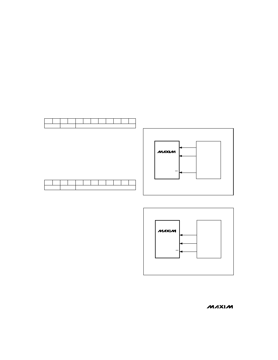
MAX534
Figure 4. Connections for Microwire
DIN
SCLK
CS
MOSI
SCK
I/0
SPI/QSPI
PORT
MAX534
Figure 5. Connections for SPI/QSPI