Detailed description – Rainbow Electronics MAX1201 User Manual
Page 8
M
A
X12
01
+5V Single-Supply, 2.2Msps, 14-Bit
Self-Calibrating ADC
8
_______________________________________________________________________________________
Detailed Description
Converter Operation
The MAX1201 is a 14-bit, monolithic, analog-to-digital
converter (ADC) capable of conversion rates up to
2.2Msps. It uses a multistage, fully differential, pipe-
lined architecture with digital error correction and self-
calibration to provide 90dB (typ) spurious-free dynamic
range at a 2.2Msps sampling rate. Its signal-to-noise
ratio, harmonic distortion, and intermodulation products
are also consistent with 14-bit accuracy up to the
Nyquist frequency. This makes the device suitable for
applications such as xDSL, digital radio, instrumenta-
tion, and imaging.
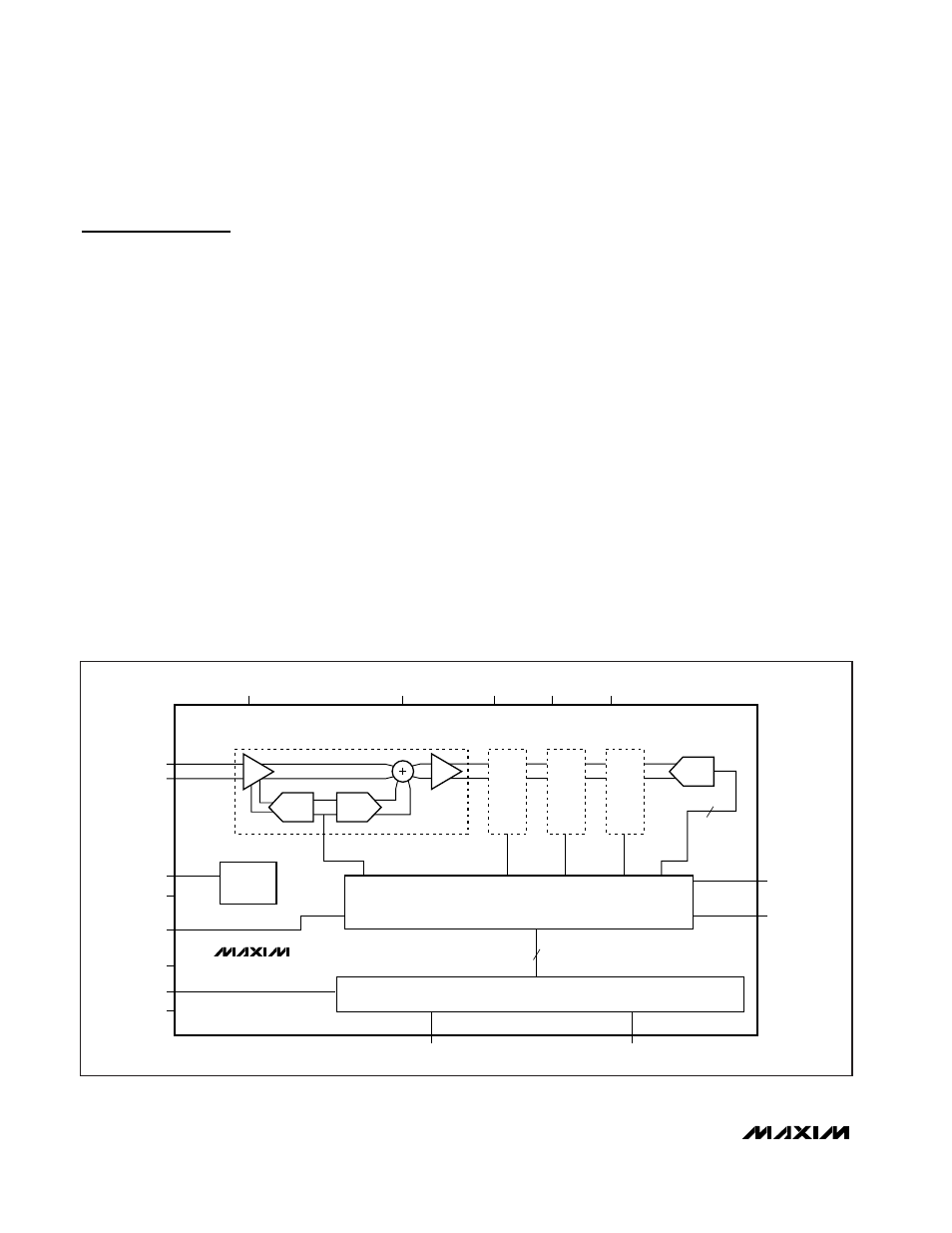
Figure 1 shows the simplified, internal structure of the
ADC. A switched-capacitor pipelined architecture is
used to digitize the signal at a high throughput rate.
The first four stages of the pipeline use a low resolution
quantizer to approximate the input signal. The multiply-
ing digital-to-analog converter (MDAC) stage is used to
subtract the quantized analog signal from the input.
The residue is then amplified with a fixed gain and
passed on to the next stage. The accuracy of the con-
verter is improved by a digital calibration algorithm
which corrects for mismatches between the capacitors
in the switched capacitor MDAC. Note that the pipeline
introduces latency of four sampling periods between
the input being sampled and the output appearing at
D13–D0. While the device can handle both single-
ended or differential inputs (see
Requirements for
Reference and Analog Signal Inputs
), the latter mode of
operation will guarantee best THD and SFDR perfor-
mance. The differential input provides the following
advantages compared to a single-ended operation:
•
Twice as much signal input span
•
Common-mode noise immunity
•
Virtual elimination of the even-order harmonics
•
Less stringent requirements on the input signal pro-
cessing amplifiers
Requirements for Reference
and Analog Signal Inputs
Fully differential switched capacitor circuits (SC) are
used for both the reference and analog inputs (Figure
2). This allows either single-ended or differential signals
to be used in the reference and/or analog signal paths.
The signal voltage on these pins (INP, INN, RFP_,
RFN_) should neither exceed the analog supply rail,
AV
DD
nor fall below ground.
STAGE1
7
DAV
INP
CM
AV
DD
RFN_
RFP_
AGND
INN
CLK
DV
DD
DGND
DRV
DD
ST_CAL
DOR
D13–D0
17
ADC
ADC
MDAC
8X
S/H
STAGE2
STAGE3
STAGE4
CORRECTION AND
CALIBRATION LOGIC
END_CAL
OE
OUTPUT DRIVERS
CLOCK
GENERATOR
MAX1201
Figure 1. Internal Block Diagram