Digital input and output characteristics – Rainbow Electronics MAX1201 User Manual
Page 4
M
A
X12
01
+5V Single-Supply, 2.2Msps, 14-Bit
Self-Calibrating ADC
4
_______________________________________________________________________________________
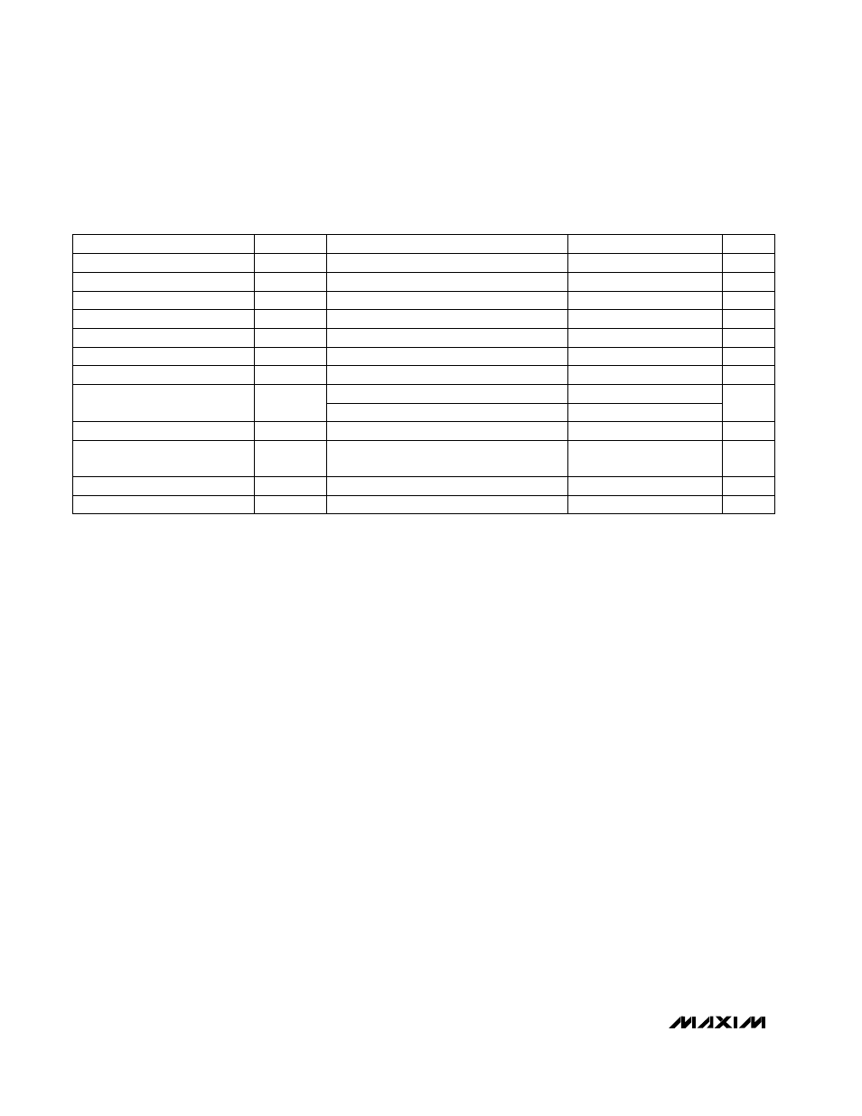
DIGITAL INPUT AND OUTPUT CHARACTERISTICS
(AV
DD
= +5V, DV
DD
= DRV
DD
= +3.3V, T
A
= T
MIN
to T
MAX
, unless otherwise noted. Typical values are at T
A
= +25°C.)
Note 1:
Reference inputs driven by operational amplifiers for Kelvin-sensed operation.
Note 2:
For unipolar mode, the analog input voltage, V
INP
, must be within 0V and V
REF
, V
INN
= V
REF
/2; where V
REF
= V
RFPS
-
V
RFNS
. For differential mode, the analog input voltages V
INP
and V
INN
must be within 0V and V
REF
; where V
REF
= V
RFPS
-
V
RFNS
. The common-mode voltage of the inputs INP and INN is V
REF
/2.
Note 3:
Minimum and maximum parameters are not tested. Guaranteed by design.
Note 4:
Input resistance varies inversely with sample rate.
Note 5:
Calibration remains valid for temperature changes within ±20°C and power-supply variations ±5%.
Note 6:
All AC specifications are shown for the differential mode.
I
SOURCE
= 200µA
V
IN_
= DV
DD
V
IN_
= 0
CONDITIONS
4.0
Input Capacitance
DV
DD
- 0.8
V
IH
0.8
V
IL
Input Low Voltage
Input High Voltage
DV
DD
DV
DD
- 0.4
- 0.03
V
OH
Output High Voltage
0.8
CLK
VIL
CLK Input Low Voltage
AV
DD
- 0.8
CLK
VIH
CLK Input High Voltage
9
C
CLK
CLK Input Capacitance
±0.1
±10
I
IN
Digital Input Current
MIN
TYP
MAX
SYMBOL
PARAMETER
I
SINK
= 1.6mA
70
400
V
OL
Output Low Voltage
±0.1
±10
I
LEAKAGE
Three-State Leakage Current
3.5
C
OUT
Three-State Output Capacitance
mV
µA
pF
pF
V
V
V
V
V
pF
µA
UNITS
±0.1
±10
V
IN_
= 0 or DV
DD
±1
±10
I
CLK
CLK Input Current
µA