Pin description (continued) – Rainbow Electronics MAX1201 User Manual
Page 7
M
A
X12
01
+5V Single-Supply, 2.2Msps, 14-Bit
Self-Calibrating ADC
_______________________________________________________________________________________
7
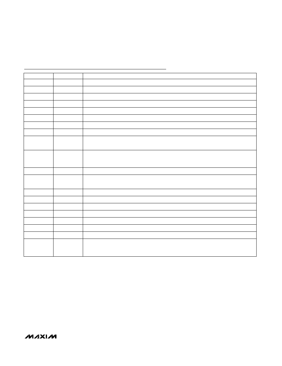
Pin Description (continued)
NAME
FUNCTION
D2
Bit 2
TEST2
Test Pin 2.
Leave unconnected.
TEST3
Test Pin 3.
Leave unconnected.
D0
Bit 0 (LSB)
D1
Bit 1
TEST1
Test Pin 1.
Leave unconnected.
DV
DD
Digital Power Supply, +3V to +5.25V.
CLK
Input Clock. Receives power from AV
DD
to reduce jitter.
DAV
Data Valid Clock. Digital Output. This clock can be used to transfer the data to a memory or any
other data-acquisition system.
OE
Output Enable: Digital Input.
OE = 0: D0–D13 and DOR are high impedance.
OE = 1: All bits are active.
TEST0
Test Pin 0.
Leave unconnected.
CM
Common-Mode Voltage. Analog Input. Drive midway between positive and negative reference
voltages.
RFPF
Positive Reference Voltage. Force Input.
RFPS
Positive Reference Voltage. Sense Input.
RFNF
Negative Reference Voltage. Force Input.
PIN
21
25
24
23
22
26
27, 30
31
32
33
34
35
36
37
38
RFNS
Negative Reference Voltage, Sense Input.
INP
Positive Input Voltage
N.C.
Not Connected. No internal connection.
39
40
41, 42
INN
Negative Input Voltage
END_CAL
Digital Output for End of Calibration.
END_CAL = 0: Calibration in progress.
END_CAL = 1: Normal conversion mode.
43
44