Applications information – Rainbow Electronics MAX1201 User Manual
Page 11
M
A
X12
01
+5V Single-Supply, 2.2Msps, 14-Bit
Self-Calibrating ADC
______________________________________________________________________________________
11
Calibration Procedure
Since the MAX1201 is based on a pipelined architec-
ture, low-resolution quantizers (“coarse ADCs”) are
used to approximate the input signal. MDACs of the
same resolution are then used to reconstruct the input
signal, which is subtracted from the input and the
residue is amplified by the switched-capacitor gain
stage. This residue is then passed on to the next stage.
The accuracy of the MAX1201 is limited by the preci-
sion of the MDAC, which is strongly dependent on the
matching of the capacitors used. The mismatch
between the capacitors is determined and stored in an
on-chip memory, which is later used during the conver-
sion of the input signal.
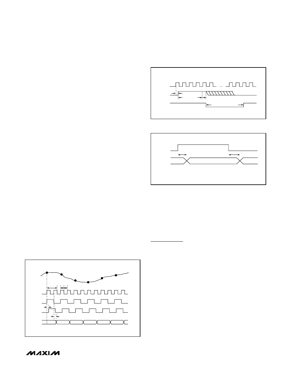
During the calibration procedure, the clock must be
running continuously. ST_CAL (start of calibration) is
initiated by a positive pulse with a minimum width of
four clock cycles but no longer than about 17,400 clock
cycles (Figure 8).
The ST_CAL input may be asynchronous with the clock,
since it is retimed internally. With ST_CAL activated,
END_CAL goes low one or two clock cycles later and
remains low until the calibration is complete. During this
period, the reference voltages must be stable to less
than 0.01%; otherwise, the calibration will be invalid.
During calibration, the analog inputs INP and INN are
not used; however, better performance is achieved if
these inputs are static. Once END_CAL goes high (indi-
cating that the calibration procedure is complete), the
ADC is ready for conversion.
Once calibrated, the MAX1201 is insensitive to small
changes (±5%) in power supply, voltage, or tempera-
ture. Following calibration, if the temperature changes
more than ±20°C, the device should be recalibrated to
maintain optimum performance.
Two’s Complement Output
The MAX1201 outputs data in two’s complement for-
mat. Table 1 shows how to convert the various full-
scale inputs into their two’s complement output codes.
Applications Information
Signal-to-Noise Ratio (SNR)
For a waveform perfectly reconstructed from digital
samples, the theoretical maximum SNR is the ratio of
full-scale analog input (RMS value) to the RMS quanti-
zation error (residual error). The ideal, theoretical mini-
mum analog-to-digital noise is caused by quantization
error only and results directly from the ADC’s resolution
(N bits):
SNR
(MAX)
= (6.02
·
N + 1.76)dB
In reality, there are other noise sources besides quanti-
zation noise including thermal noise, reference noise,
clock jitter, etc. Therefore, SNR is computed by taking
the ratio of the RMS signal to the RMS noise which
includes all spectral components minus the fundamen-
tal, the first nine harmonics, and the DC offset.
t
S
t
CH
t
CL
N
CLK
AIN
SAMPLE
CLOCK
DAV
N-3
N-2
N-1
N
N+1
D0–D13
N+1
N+2
N+3
N+4
N+5
t
OD
CLK
ST_CAL
END_CAL
MIN 4 t
CLK
~17,400 CLK CYCLES
Figure 8. Timing for Start and End of Calibration
Figure 7. Main Timing Diagram
Z
Z = HIGH IMPEDANCE (THREE-STATED)
Z
DOR
D0–D13
OE
t
AC
t
REL
Figure 9. Timing for Bus Access and Bus Relinquish—
Controlled by Output Enable (OE)