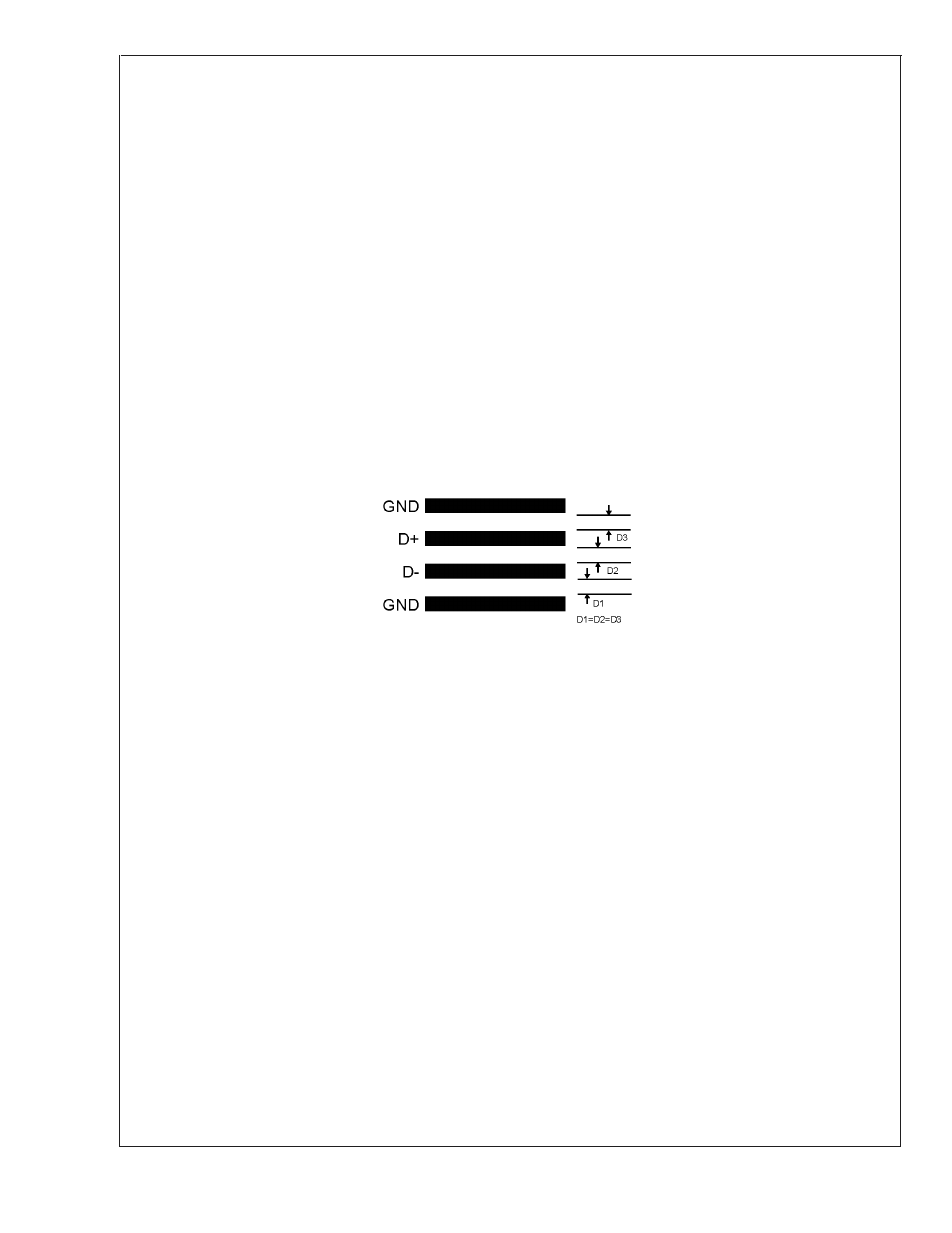
5 pcb layout recommendations for minimizing noise, Figure 9. recommended diode trace layout, Functional description – Rainbow Electronics LM87 User Manual
Page 18
Functional Description
(Continued)
η from part to part. As an example, assume a temperature
sensor has an accuracy specification of
±
3˚C at room tem-
perature of 25˚C and the process used to manufacture the
diode has a non-ideality variation of
±
1%. The resulting
accuracy of the temperature sensor at room temperature will
be:
T
ACC
=
±
3˚C + (
±
1% of 298˚K) =
±
6˚C
.
The additional inaccuracy in the temperature measurement
caused by
η, can be eliminated if each temperature sensor is
calibrated with the remote diode that it will be paired with.
8.5 PCB Layout Recommendations for Minimizing
Noise
In a noisy environment, such as a processor mother board,
layout considerations are very critical. Noise induced on
traces running between the remote temperature diode sen-
sor and the LM87 can cause temperature conversion errors.
The following guidelines should be followed:
1.
Place a 0.1 µF power supply bypass capacitor as close
as possible to the V
CC
pin and the recommended 2.2 nF
capacitor as close as possible to the D+ and D− pins.
Make sure the traces to the 2.2 nF capacitor are
matched.
2.
Ideally, the LM87 should be placed within 10 cm of the
Processor diode pins with the traces being as straight,
short and identical as possible.
3.
Diode traces should be surrounded by a GND guard ring
to either side, above and below if possible. This GND
guard should not be between the D+ and D− lines. In the
event that noise does couple to the diode lines it would
be ideal if it is coupled common mode. That is equally to
the D+ and D− lines.
4.
Avoid routing diode traces in close proximity to power
supply switching or filtering inductors.
5.
Avoid running diode traces close to or parallel to high
speed digital and bus lines. Diode traces should be kept
at least 2 cm. apart from the high speed digital traces.
6.
If it is necessary to cross high speed digital traces, the
diode traces and the high speed digital traces should
cross at a 90 degree angle.
7.
The ideal place to connect the LM87’s GND pin is as
close as possible to the Processors GND associated
with the sense diode. For the Pentium II this would be
pin A14.
Noise on the digital lines, overshoot greater than V
CC
and
undershoot less than GND, may prevent successful SMBus
communication with the LM87. SMBus no acknowledge is
the most common symptom, causing unnecessary traffic on
the bus. Although, the SMBus maximum frequency of com-
munication is rather low (400 kHz max) care still needs to be
taken to ensure proper termination within a system with
multiple parts on the bus and long printed circuit board
traces. A lowpass filter, in series with the SMBCLK and
SMBData, has been added internally to the LM87 for noise
immunity. The lowpass filter has a typical cutoff frequency of
20MHz. Additional noise immunity can be achieved by plac-
ing a resistor (4.7k to 5.1k Ohms) in series with the SMBCLK
input as close to the LM87 as possible. This resistance, in
conjunction with the IC input capacitance, reduces high fre-
quency noise seen at the SMBCLK input and increases the
reliability of communications.
10099535
FIGURE 9. Recommended Diode Trace Layout
LM87
www.national.com
18