Design procedure – Rainbow Electronics MAX1801 User Manual
Page 9
MAX1801
Digital Camera Step-Up Slave
DC-DC Controller
_______________________________________________________________________________________
9
Shutdown
Set V
DCON
less than 0.35V to place the MAX1801 in
sleep mode, which drops the supply current to 5µA. To
reduce the supply current to 10nA, place the MAX1801
in shutdown by setting V
REF
below 0.4V. The MAX1801
enters soft-start when both V
DCON
and V
REF
are at nor-
mal levels.
Short-Circuit Protection
The MAX1801 has a fault protection feature that pre-
vents damage to transformer-coupled or SEPIC circuits
due to an output short circuit. If the output voltage
drops out of regulation, the voltage at COMP is
clamped at 2.7V. If this condition is maintained for 1024
oscillator clock periods at any time following soft-start,
the MAX1801 is disabled to prevent excessive output
current. Restart the controller by cycling the voltage at
DCON or IN to GND and back to a normal state. For a
step-up application, short-circuit current is not limited,
due to the DC current path through the inductor and
output rectifier to the short circuit. If short-circuit protec-
tion is required in a step-up configuration, a protection
device such as a fuse must be used to limit short-circuit
current.
Design Procedure
The MAX1801 can operate in a number of DC-DC con-
verter configurations, including step-up, SEPIC, and fly-
back. The following design discussions are limited to
the step-up configuration shown in Figure 1; SEPIC and
flyback examples are discussed in the Applications
Information section.
Switching Frequency
The MAX1801 switching frequency is set by the
MAX1800 or MAX1802 master converter (refer to the
appropriate data sheet for the design procedure).
Choose a switching frequency to optimize external
component size or efficiency for the particular
MAX1801 application. Typically, switching frequencies
between 400kHz and 500kHz offer a good balance
between component size and efficiency—higher fre-
quencies generally allow smaller components, and
lower frequencies give better conversion efficiency.
Setting the Output Voltages
Set the MAX1801 output voltage by connecting a resis-
tive voltage-divider from the output to FB as shown in
Figure 1. The FB input bias current is less than 100nA,
so choose R2 to be 100k
Ω to minimize the effect of
input bias current at FB. Choose R1 according to the
relation:
where V
FB
is 1.25V, the regulation set point for the
MAX1801.
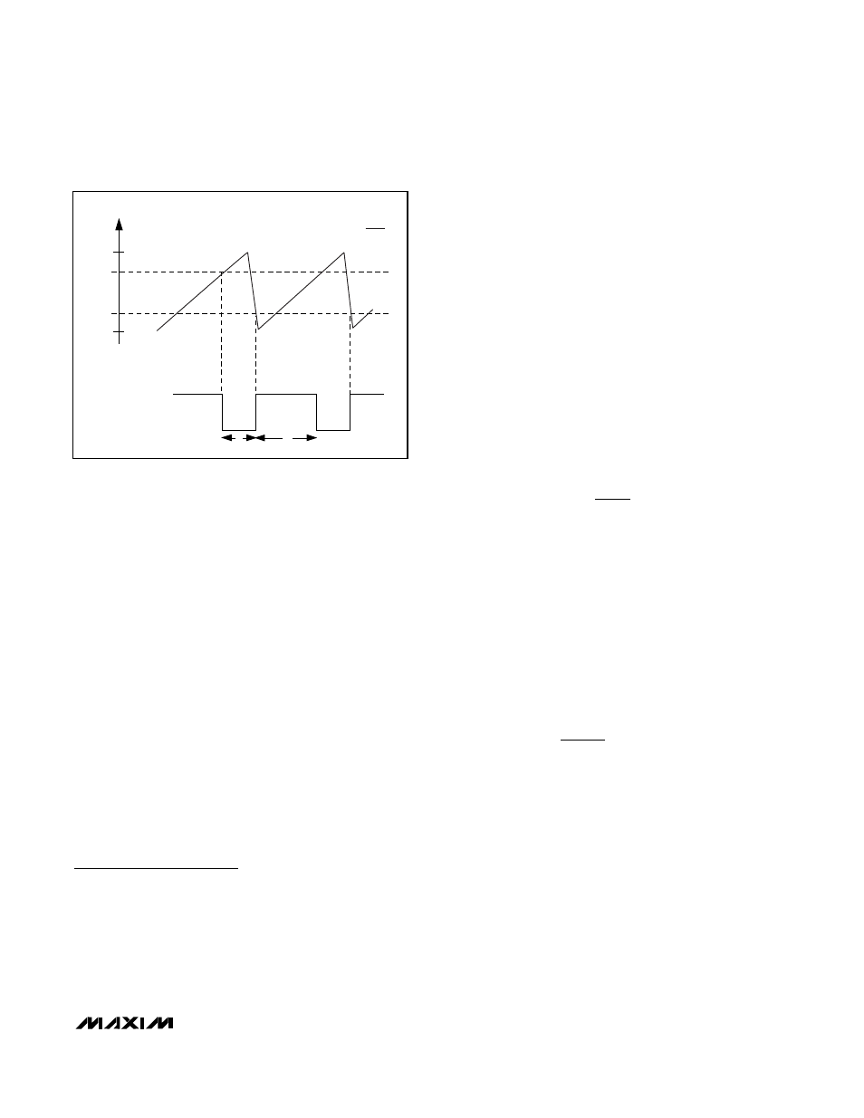
Setting the Maximum Duty Cycle
The master oscillator signal at OSC and the voltage at
DCON are used to generate the internal clock signal
(CLK in Figure 2). The internal clock’s falling edge
occurs when V
OSC
exceeds V
DCON
, the voltage at
DCON set by a resistive voltage-divider. The internal
clock’s rising edge occurs when V
OSC
falls below
0.25V (Figure 3). The maximum duty cycle can be
approximated by the equation:
where f
OSC
and t
FALL
are the oscillator frequency (in
Hz) and the fall time (typically 100ns), respectively.
At 100kHz, the adjustable maximum duty-cycle range is
typically 28% to 92% (see Maximum Duty Cycle vs.
V
DCON
in the Typical Operating Characteristics). The
maximum duty cycle typically defaults to 78% at 100kHz
if V
DCON
is at or above the voltage at V
REF
(1.25V), and
the controller shuts down if V
DCON
is less than 0.4V. If a
resistive voltage-divider is used at DCON, shut down the
MAX1801 by pulling DCON low with an open-drain sig-
nal from an external transistor. Drive DCON with appro-
priate logic levels to turn the MAX1801 on and off if the
default duty-cycle limit is used.
D
R
R
R
f
t
MAX
OSC FALL
=
+
−
(
)
4
3
4
1
R
R
V
V
OUT
FB
1
1
2
=
−
t
1
t
2
1.25
V
OSC
(V)
V
DCON
0.25
0
CLK
t
2
t
1
+ t
2
D
MAX
=
Figure 3. Setting the Maximum Duty Cycle