Chip information, Pin configuration – Rainbow Electronics MAX1801 User Manual
Page 15
MAX1801
Digital Camera Step-Up Slave
DC-DC Controller
______________________________________________________________________________________
15
FB
COMP
DCON
1
2
8
7
DL
IN
GND
REF
OSC
SOT23-8
TOP VIEW
3
4
6
5
MAX1801
Chip Information
TRANSISTOR COUNT: 1130
Pin Configuration
Designing a PC Board
A good PC board layout is important to achieve optimal
performance from the MAX1801. Poor design can cause
excessive conducted and/or radiated noise, both of
which can cause instability and/or regulation errors.
Conductors carrying discontinuous currents should be
kept as short as possible, and conductors carrying
high currents should be made as wide as possible. A
separate low-noise ground plane containing the refer-
ence and signal grounds should connect only to the
power-ground plane at one point to minimize the
effects of power-ground currents.
Keep the voltage feedback network very close to the
IC, preferably within 0.2in (5mm) of the FB pin. Nodes
with high dv/dt (switching nodes) should be kept as
small as possible and should be kept away from high-
impedance nodes such as FB.
Circuit-board layouts that are susceptible to electrical
noise can require a lowpass RC filter at OSC and
bypassing at REF and IN. If an RC filter is used at OSC,
the pole frequency should be at least 20 times larger
than the oscillator frequency to prevent distortion of the
OSC signal. To ensure minimal loading of the master
oscillator, which would cause an oscillator frequency
shift, choose a filter capacitor smaller than C
OSC
/(100
N), where C
OSC
is the timing capacitor for the master
oscillator and N is the number of MAX1801 slaves con-
nected to the master. Then choose R
FILTER
= 1/(40
π
f
OSC
C
FILTER
).
If bypass capacitors are required on IN and REF, use
0.1µF ceramic capacitors because of their low imped-
ance at high frequencies. The bypass and filter compo-
nents should be placed within 5mm (0.2in) of the
MAX1801 pins.
Refer to the MAX1800 evaluation kit (EV kit) or
MAX1802 EV kit data sheets for full PC board exam-
ples.
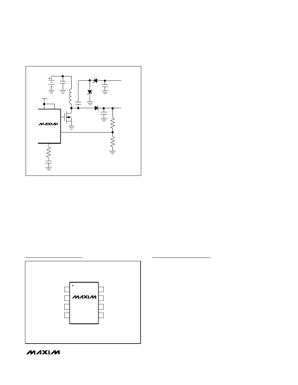
MAX1801
V
OUT
-
V
OUT
+
D
3
D
2
D
1
C
3
C
2
R
1
R
2
R
C
G
C
C
1
Q
1
L
INPUT
MAIN
ON
COMP
DCON
EXT
FB
Figure 8. Auxiliary Controller, Charge-Pump Configuration