Pin description, Typical operating characteristics (continued) – Rainbow Electronics MAX1801 User Manual
Page 6
MAX1801
Digital Camera Step-Up Slave
DC-DC Controller
6
_______________________________________________________________________________________
Pin Description
PIN
NAME
FUNCTION
1
OSC
Oscillator Input. Connect OSC to OSC of the MAX1800 or MAX1802. The oscillator frequency must
be between 100kHz and 1MHz.
2
GND
Ground
3
REF
1.25V Reference Input. Connect REF to REF of the MAX1800 or MAX1802. REF must be above 1V
for the controller to turn on. Bypass REF to GND with a 0.1µF or greater capacitor.
4
DCON
Maximum Duty-Cycle Control Input. Connect to REF or IN to set the default maximum duty cycle.
Connect a resistive voltage-divider from REF to DCON to set the maximum duty cycle between 40%
and 90%. Pull DCON below 0.35V to turn the controller off.
5
COMP
Controller Compensation. Output of transconductance error amplifier. Connect a series resistor and
capacitor to GND to compensate the control loop. See Compensation Design.
6
FB
Controller Feedback Input. Connect a feedback resistive voltage-divider from the output to FB to
set the output voltage. Regulation voltage is V
REF
(1.25V).
7
IN
IC Supply Bias Input. Bypass IN to GND with a 0.1µF or greater ceramic capacitor. Supply range is
2.7V to 5.5V.
8
DL
External MOSFET Gate Drive Output. DL swings between IN and GND with typical 500mA drive
current. Connect DL to the gate of the external switching N-channel MOSFET.
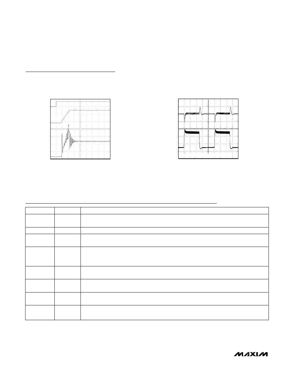
STARTUP RESPONSE
MAX1801 toc10
V
DCON
5V/div
V
OUT
2V/div
I
IN
0.5A/div
1ms/div
OV
OV
OA
LOAD TRANSIENT RESPONSE
MAX1801 toc11
V
OUT
100mV/div
(AC-COUPLED)
400
µs/div
I
LOAD
0.2A/div
V
IN
= =+2.4V, V
OUT
= +5V, f
OSC
= 500kHz
100mA
OA
500mA
Typical Operating Characteristics (continued)
(Circuit of Figure 1, T
A
= +25°C, unless otherwise noted.)