Max152, 3v, 8-bit adc with 1µa power-down – Rainbow Electronics MAX152 User Manual
Page 8
MAX152
A minimum acquisition time (tP) is required from INT
going low to the start of another conversion (
WR going
low).
Options for reading data from the converter include the
following:
Using Internal Delay
The µP waits for the
INT output to go low before read-
ing the data (Figure 4).
INT goes low after the rising
edge of
WR, indicating that the conversion is complete
and the result is available in the output latch. With
CS
low, data outputs D0-D7 can be accessed by pulling
RD low. INT is then reset by the rising edge of CS or
RD.
Fastest Conversion: Reading Before Delay
An external method of controlling the conversion time is
shown in Figure 5. The internally generated delay
tINTL varies slightly with temperature and supply volt-
age, and can be overridden with
RD to achieve the
fastest conversion time.
RD is brought low after the ris-
ing edge of
WR, but before INT goes low. This com-
pletes the conversion and enables the output buffers
(D0-D7) that contain the conversion result.
INT also
goes low after the falling edge of
RD and is reset on the
rising edge of
RD or CS. The total conversion time is
therefore: tCWR = tWR (600ns) + tRD (800ns) + tACC1
(400ns) = 1800ns.
Stand-Alone Operation
Besides the two standard WR-RD mode options, stand-
alone operation can be achieved by connecting
CS
and
RD low (Figure 6). A conversion is initiated by
pulling
WR low. Output data can be read by either
edge of the next
WR pulse.
+3V, 8-Bit ADC with 1µA Power-Down
8
_______________________________________________________________________________________
tP
tINTL
WR
INT
NEW DATA
tWR
tIHWR
tID
OLD DATA
D0-D7
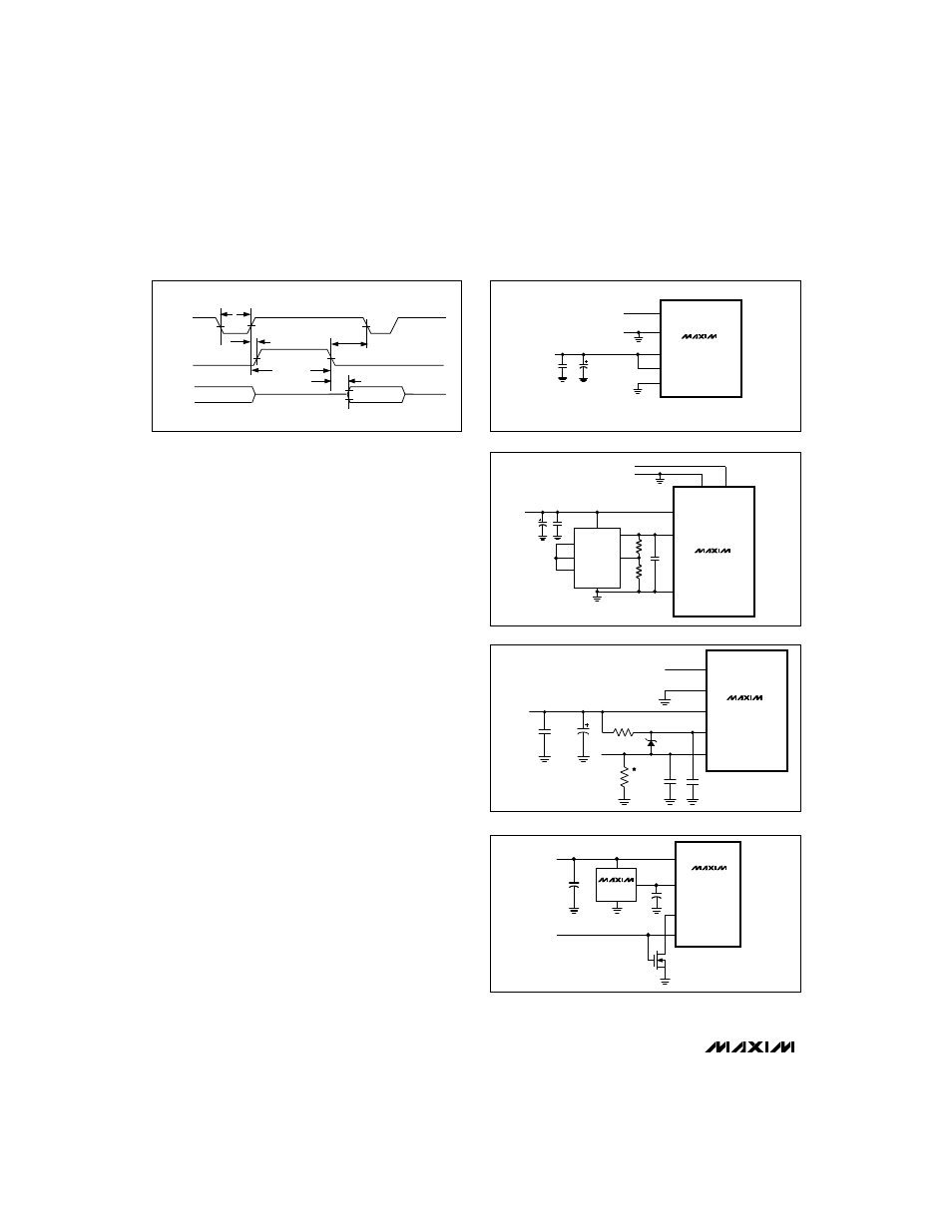
Figure 6. Stand-Alone Mode Timing (
CS
=
RD
= 0) (MODE = 1)
VREF-
MAX152
VDD
0.1µF
VIN
VREF+
VIN+
VIN-
GND
+3V
1
10
20
12
11
4.7µF
Figure 7a. Power Supply as Reference
+3V
0.1
µF
4
VREF-
MAX152
VREF+
VIN
8
1
3
7
0.1
µF
4.7
µF
2
6
GND
VDD
10
1
20
12
11
+2.5V
34.8k
3.01k
LM10
VIN+
VIN-
Figure 7b. External Reference, +2.5V Full Scale
+3V
0.1µF
12
VREF-
MAX152
VREF+
VIN
10
1
20
11
0.1µF
4.7µF
GND
VDD
0.1µF
VIN-
1.2V
VIN+
*CURRENT PATH MUST STILL
EXIST FROM VIN- TO GND.
Figure 7c. Input Not Referenced to GND
+3V
PWRDN
C1
2.2µF
MTD3055EL
N
MAX152
VREF-
VDD
VREF+
PWRDN
MAX872
+
Figure 7d. An N-channel MOSFET switches off the reference
load during power-down.