Electrical characteristics, Absolute maximum ratings – Rainbow Electronics MAX152 User Manual
Page 2
MAX152
+3V, 8-Bit ADC with 1µA Power-Down
2
_______________________________________________________________________________________
VDD to GND .............................................................-0.3V to +7V
VSS to GND ..............................................................+0.3V to -7V
Digital Input Voltage to GND ........................-0.3V, (VDD + 0.3V)
Digital Output Voltage to GND .....................-0.3V, (VDD + 0.3V)
VREF+ to GND................................(VSS - 0.3V) to (VDD + 0.3V)
VREF- to GND.................................(VSS - 0.3V) to (VDD + 0.3V)
VIN to GND .....................................(VSS - 0.3V) to (VDD + 0.3V)
Continuous Power Dissipation (TA = +70°C)
Plastic DIP (derate 11.11mW/°C above +70°C) ..........889mW
Wide SO (derate 10.00mW/°C above +70°C)..............800mW
SSOP (derate 8.00mW/°C above +70°C) ....................640mW
CERDIP (derate 11.11mW/°C above +70°C) ...............889mW
Operating Temperature Ranges:
MAX152C__ ........................................................0°C to +70°C
MAX152E__ .....................................................-40°C to +85°C
MAX152MJP ..................................................-55°C to +125°C
Storage Temperature Range .............................-65°C to +150°C
Lead Temperature (soldering, 10sec) .............................+300°C
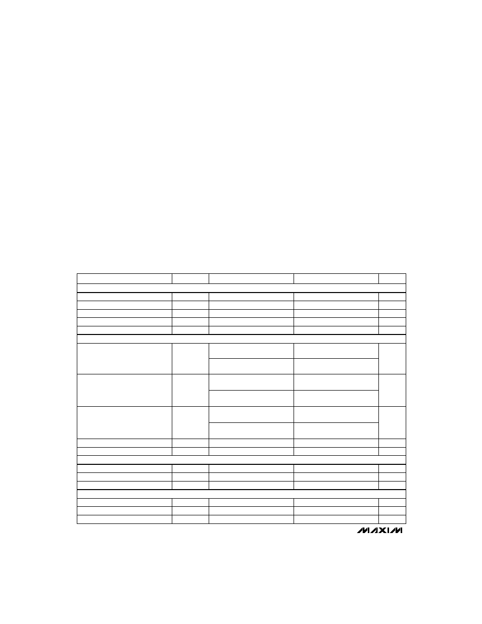
ELECTRICAL CHARACTERISTICS
(Unipolar input range, V
DD
= 3.0V to 3.6V, GND = 0V, V
SS
= GND, VREF+ = 3.0V, VREF- = GND, specifications are given for RD
mode (pin 7 = GND), T
A
= T
MIN
to T
MAX
, unless otherwise noted.)
Stresses beyond those listed under “Absolute Maximum Ratings” may cause permanent damage to the device. These are stress ratings only, and functional
operation of the device at these or any other conditions beyond those indicated in the operational sections of the specifications is not implied. Exposure to
absolute maximum rating conditions for extended periods may affect device reliability.
PARAMETER
SYMBOL
CONDITIONS
UNITS
Resolution
N
Bits
Total Unadjusted Error
TUE
Unipolar range
LSB
Differential Nonlinearity
DNL
No-missing-codes guaranteed
LSB
Zero-Code Error (Note 2)
Unipolar and bipolar modes
LSB
Full-Scale Error (Note 2)
Unipolar and bipolar modes
LSB
S/(N+D)
MAX152C/E, f
SAMPLE
=
400kHz, f
IN
= 30.273kHz
dB
THD
dB
Spurious-Free Dynamic Range
dB
Input Full-Power Bandwidth
V
IN
= 3.0V
p-p
MHz
Maximum Input Slew Rate, Tracking
V/µs
Input Voltage Range
V
IN
V
Input Leakage Current
I
IN
V
SS
< V
IN
< V
DD
µA
Input Capacitance
C
IN
pF
Reference Resistance
RREF
k
Ω
VREF+ Input Voltage Range
V
VREF- Input Voltage Range
V
Signal-to-Noise Plus
Distortion Ratio
Total Harmonic Distortion
MAX152M, f
SAMPLE
= 340kHz,
f
IN
= 30.725kHz
MAX152C/E, f
SAMPLE
=
400kHz, f
IN
= 30.273kHz
MAX152M, f
SAMPLE
= 340kHz,
f
IN
= 30.725kHz
ABSOLUTE MAXIMUM RATINGS
MAX152C/E, f
SAMPLE
=
400kHz, f
IN
= 30.273kHz
MAX152M, f
SAMPLE
= 340kHz,
f
IN
= 30.725kHz
MIN
TYP
MAX
8
±1
±1
±1
±1
-50
-50
50
50
0.3
0.28
0.5
VREF-
VREF+
±3
22
1
2
4
VREF- V
DD
V
SS
VREF+
45
45
DYNAMIC PERFORMANCE
(Note 3)
ACCURACY
(Note 1)
ANALOG INPUT
REFERENCE INPUT