Digital interface, Read mode (mode = 0), Write-read mode (mode = 1) – Rainbow Electronics MAX152 User Manual
Page 7
MAX152
+3V, 8-Bit ADC with 1µA Power-Down
_______________________________________________________________________________________
7
Once the MAX152 is in power-down mode, lowest sup-
ply current is drawn with MODE low (RD mode) due to
an internal pull-down resistor at this pin. In addition, for
minimum current consumption, other digital inputs
should remain high in power-down. Refer to the
Reference section for information on reducing refer-
ence current during power-down.
___________________Digital Interface
The MAX152 has two basic interface modes set by the
status of the MODE input pin. When MODE is low, the
converter is in the RD mode; when MODE is high, the
converter is set up for the WR-RD mode.
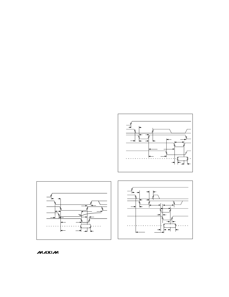
Read Mode (MODE = 0)
In RD mode, conversion control and data access are
controlled by the
RD input (Figure 3). The comparator
inputs track the analog input voltage for the duration of
tP. A conversion is initiated by driving RD low. With µPs
that can be forced into a wait state, hold
RD low until
output data appears. The µP starts the conversion,
waits, and then reads data with a single read instruction.
WR/RDY is configured as a status output (RDY) in RD
mode, where it can drive the ready or wait input of a
µP. RDY is an open-collector output (with no internal
pull-up) that goes low after the falling edge of
CS and
goes high at the end of the conversion. If not used, the
WR/RDY pin can be left unconnected. The INT output
goes low at the end of the conversion and returns high
on the rising edge of
CS or RD.
Write-Read Mode (MODE = 1)
Figures 4 and 5 show the operating sequence for the
write-read (WR-RD) mode. The comparator inputs
track the analog input voltage for the duration of tP.
The conversion is initiated by a falling edge of
WR.
When
WR returns high, the 4 MSBs' flash result is
latched into the output buffers and the 4 LSBs' conver-
sion begins.
INT goes low, indicating conversion end,
and the lower 4 data bits are latched into the output
buffers. The data is then accessible after
RD goes low
(see
Timing Characteristics).
tUP
tCSS
tP
tCSH
tDH
tREAD2
tRD
D0-D7
RD
WR
CS
PWRDN
INT
VALID DATA
tINTL
tACC2
tWR
Figure 4. WR-RD Mode Timing (t
RD
> t
INTL
) (MODE = 1)
tUP
tCSS
tP
tCSH
tDH
tREAD1
tRD
RD
WR
CS
PWRDN
INT
VALID DATA
tINTH
tWR
tACC1
tCWR
tRI
Figure 5. WR-RD Mode Timing (t
RD
< t
INTL
),
Fastest Operating
Mode (MODE = 1)
tUP
tCSS
tRDY
WITH EXTERNAL
PULL-UP
tP
tCSH
tINTH
tDH
tCRD
tACCO
D0-D7
RDY
RD
CS
PWRDN
INT
VALID DATA
Figure 3. RD Mode Timing (MODE = 0)