Converter operation, Power-down mode – Rainbow Electronics MAX152 User Manual
Page 6
MAX152
+3V, 8-Bit ADC with 1µA Power-Down
6
_______________________________________________________________________________________
PIN
NAME
FUNCTION
1
V
IN
2
D0
Three-State Data Output (LSB)
3-5
D1-D3
Three-State Data Outputs
6
WR/RDY
7
MODE
8
RD
9
INT
10
GND
Ground
11
VREF-
12
VREF+
13
CS
14-16
D4-D6
Three-State Data Outputs
17
D7
Three-State Data Output (MSB)
18
PWRDN
19
V
SS
20
V
DD
Positive Supply, +3V.
Analog Input. Range is
VREF-
≤
V
IN
≤
VREF+.
Write Control Input/Ready Status
Output*
Mode Selection Input is internally
pulled low with a 15µA current source.
MODE = 0 activates read mode
MODE = 1 activates write-read mode*
Read Input must be low to access
data.*
Interrupt Output goes low to indicate
end of conversion.*
Lower limit of reference span. Sets the
zero-code voltage. Range is
V
SS
≤
VREF- < VREF+.
Upper limit to reference span. Sets the
full-scale input voltage. Range is
VREF- < VREF+
≤
V
DD
.
Chip-Select Input must be low for the
device recognize
WR or RD inputs.
Powerdown Input reduces supply
current when low.
Negative Supply. Unipolar: VSS = 0V,
Bipolar: V
SS
= -3V.
____________________Pin Description
_______________Detailed Description
Converter Operation
The MAX152 uses a half-flash conversion technique
(see
Functional Diagram) in which two 4-bit flash ADC
sections achieve an 8-bit result. Using 15 compara-
tors, the flash ADC compares the unknown input volt-
age to the reference ladder and provides the upper 4
data bits.
An internal digital-to-analog converter (DAC) uses the
4 most significant bits (MSBs) to generate the analog
result from the first flash conversion and a residue volt-
age that is the difference between the unknown input
and the DAC voltage. The residue is then compared
again with the flash comparators to obtain the lower 4
data bits (LSBs).
The MAX152 is characterized for operation between
+3.0V and +3.6V. Conversion times decrease as the
supply voltage increases. The supply current decreas-
es rapidly with decreasing supply voltage. (See
Typical Operating Characteristics.)
Power-Down Mode
In burst-mode or low sample-rate applications, the
MAX152 can be shut down between conversions,
reducing supply current to microamp levels (see
Typical Operating Characteristics). A logic low on the
PWRDN pin shuts the device down, reducing supply
current to typically 1µA when powered from a single 3V
supply. A logic high on
PWRDN wakes up the
MAX152. A new conversion can be started within
900ns of the
PWRDN pin being driven high (this
includes both the power-up delay and the track/hold
acquisition time). If power-down mode is not required,
connect
PWRDN to V
DD
.
*See
Digital Inferface
Section.
DATA
OUTPUTS
DATA
OUTPUTS
C
L
3k
C
L
A. HIGH-Z TO VOH
B. HIGH-Z TO VOL
3k
VDD
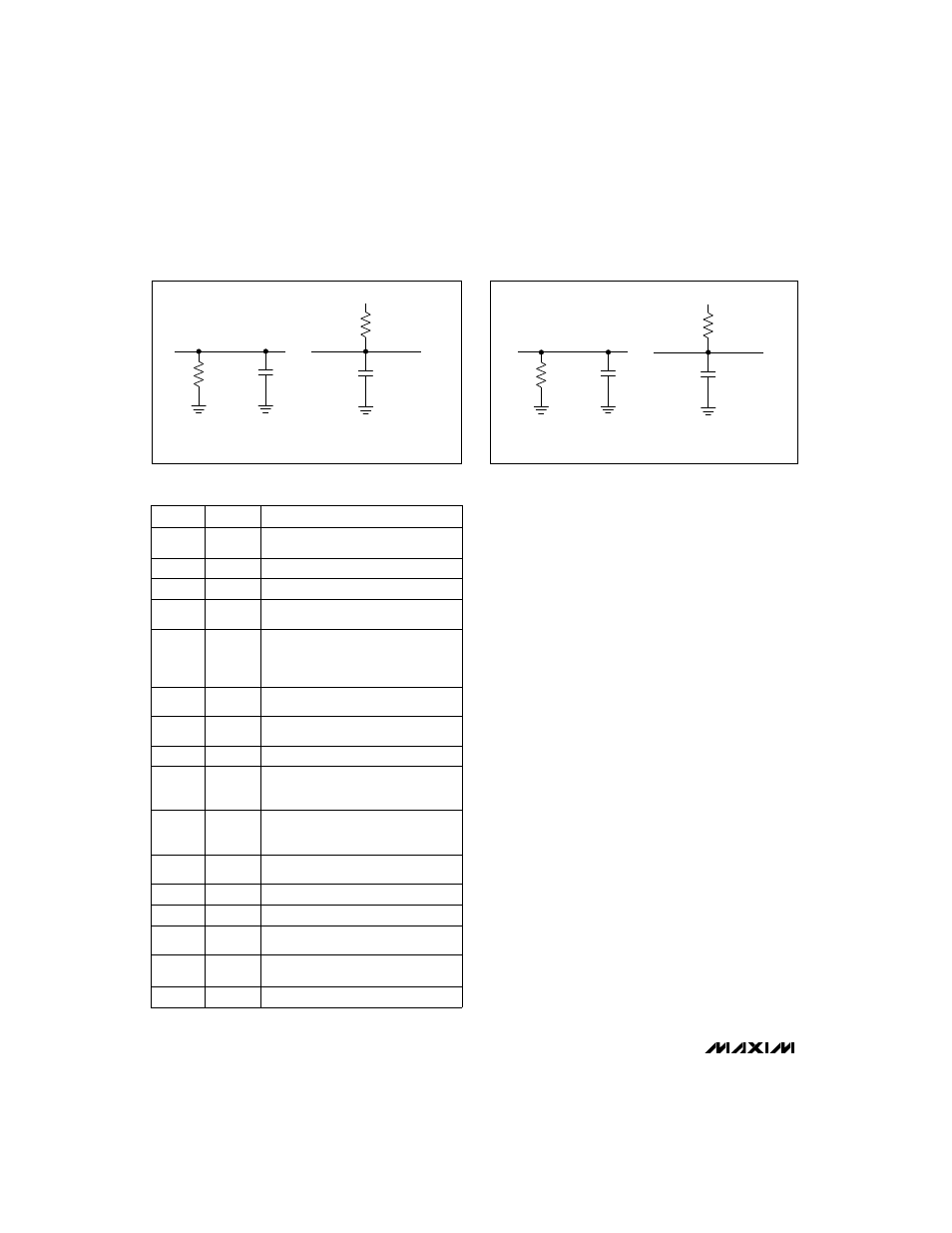
Figure 1. Load Circuits for Data-Access Time Test
DATA
OUTPUTS
10pF
3k
10pF
A. VOH TO HIGH-Z
B. VOL TO HIGH-Z
3k
VDD
DATA
OUTPUTS
Figure 2. Load Circuits for Data-Hold TIme Test