Timing characteristics – Rainbow Electronics MAX152 User Manual
Page 4
_________________________________________________________________________________________
MAX152
+3V, 8-Bit ADC with 1µA Power-Down
4
_______________________________________________________________________________________
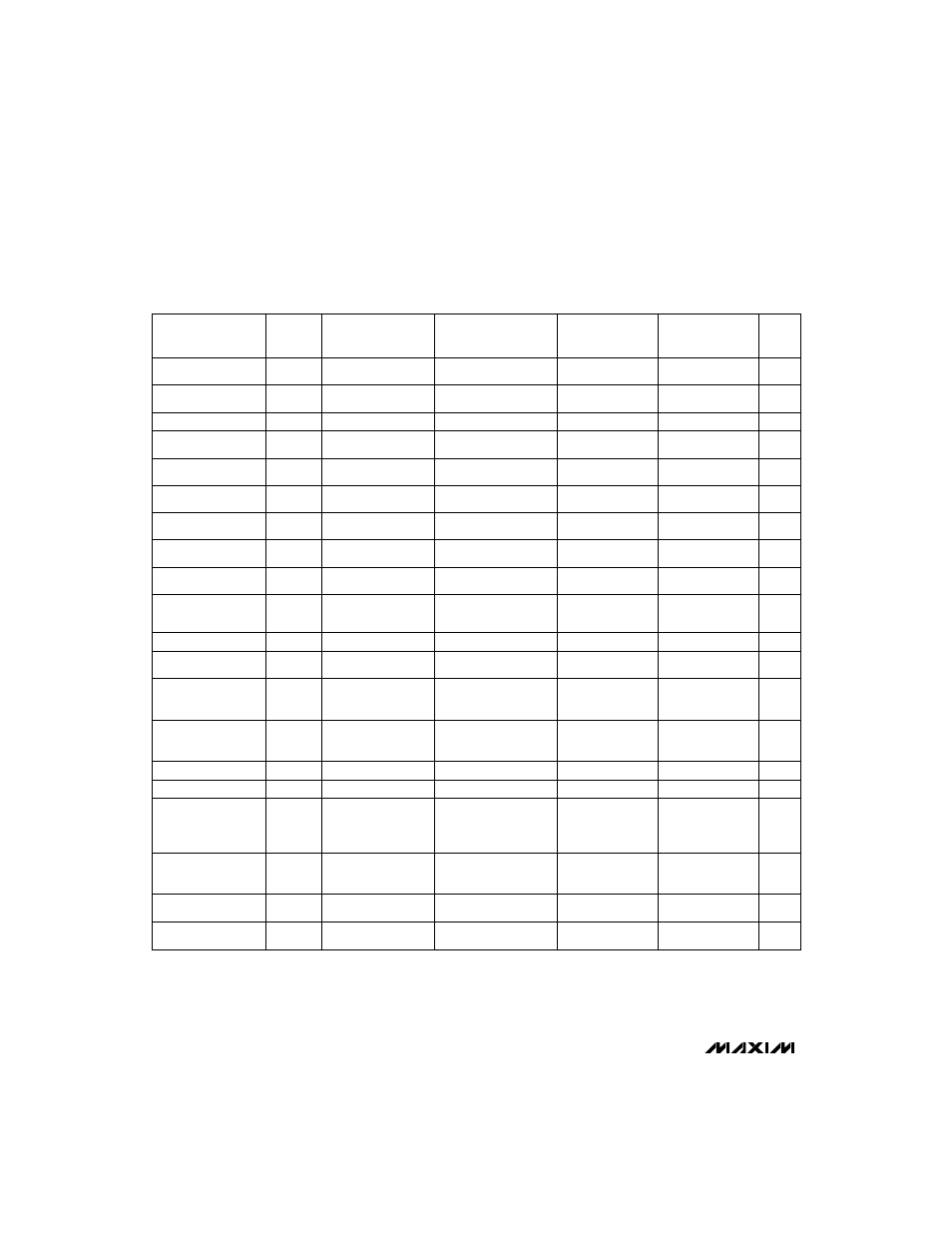
PARAMETER
SYMBOL
CONDITIONS
MAX152C/E
T
A
= T
MIN
to T
MAX
MIN
MAX
MAX152M
T
A
= T
MIN
to T
MAX
MIN
MAX
UNITS
WR Pulse Width
t
WR
0.6
10
0.66
10
0.8
10
µs
Delay Time Between
WR and RD Pulses
t
RD
0.8
0.9
1.0
µs
RD Pulse Width
t
READ1
400
500
600
ns
t
ACC1
400
500
600
ns
RD to INT Delay
t
RI
300
340
400
ns
t
CWR
t
RD
< t
INTL
,
C
L
= 100pF
1.8
2.06
2.4
µs
Conversion Time
(RD Mode)
t
CRD
2.0
2.3
2.6
µs
Power-Up Time
t
UP
0.9
1.2
1.4
µs
CS to RD,WR
Setup Time
t
CSS
0
0
0
ns
CS to RD,WR
Hold Time
t
CSH
0
0
0
ns
CS to RDY
Delay
t
RDY
C
L
= 50pF,
R
L
= 5.1k
Ω
to V
DD
100
120
140
ns
WR to INT Delay
t
INTL
C
L
= 50pF
0.7
1.45
1.6
1.8
RD Pulse Width
t
READ2
WR-RD mode,
t
RD
> t
INTL
,
determined by t
ACC2
(Figure 5)
180
220
250
ns
Data Access Time
(Note 7)
t
ACC2
180
220
250
ns
WR to INT Delay
t
IHWR
180
200
240
ns
Data Access Time
After
INT (Note 7)
t
ID
Stand-alone mode,
C
L
= 100pF
100
130
150
ns
Data Access Time
(RD Mode) (Note 7)
t
ACC0
C
L
= 100pF
t
CRD
+100
t
CRD
+150
ns
RD to INT Delay
(RD Mode)
t
INTH
C
L
= 50pF
100
160
170
180
ns
Data Hold Time
(Note 8)
t
DH
100
130
150
ns
t
P
450
600
700
ns
ALL GRADES
T
A
= +25°C
MIN
TYP
MAX
Conversion Time
(WR-RD Mode)
Delay Time Between
Conversions
Data Access Time
(Note 7)
WR-RD mode,
determined by t
ACC1
(Figure 6)
WR-RD mode,
t
RD
< t
INTL
, C
L
= 100pF
(Figure 6)
WR-RD mode,
t
RD
< t
INTL
, C
L
= 100pF
(Figure 5)
t
CRD
+130
µs
TIMING CHARACTERISTICS
(Unipolar input range, V
DD
= 3V, V
SS
= 0V, T
A
= +25°C, unless otherwise noted.) (Note 6)
Note 6:
Input control signals are specified with tr = tf = 5ns, 10% to 90% of +3.0V, and timed from a voltage level of 1.3V. Timing
delays get shorter at higher supply voltages. See the Converson Time vs. Supply Voltage graph in the
Typical Operating
Characteristics
to extrapolate timing delays at other power-supply voltages.
Note 7:
See Figure 1 for load circuit. Parameter defined as the time required for the output to cross 0.66V or 2.0V.
Note 8:
See Figure 2 for load circuit. Parameter defined as the time required for the data lines to change 0.5V.
Stand-alone mode,
C
L
= 50pF