Table 1. output coding – Rainbow Electronics MAX555 User Manual
Page 7
MAX555
300Msps, 12-Bit DAC with
Complementary Voltage Outputs
_______________________________________________________________________________________
7
The DAC’s control amplifier has a typical open-loop volt-
age gain of 85dB, and its gain-magnitude bandwidth is
flat up to 10MHz. When the control amplifier is not being
used for high-speed multiplying applications, it is recom-
mended that a 0.4µF capacitor be connected from LBIAS
to AV
EE
to increase control-amplifier stability and reduce
current-source noise.
Timing Information
The MAX555 features a differential ECL clock input with
selective transparent operation (BYPASS = 1). It is possi-
ble to drive the MAX555 clock single-ended if desired by
tying the CLK input to an external voltage of -1.3V (ECL
V
BB
). However, using a differential clock provides greater
noise immunity and improved dynamic performance.
In clocked mode (BYPASS = 0), when the clock line is
low, the slave register is locked out and information on
the digital inputs is permitted to enter the master regis-
ter. The clock transition from low to high locks the mas-
ter register in its present state and ignores further
changes on the digital inputs. This transition simultane-
ously transfers the contents of the master register to the
slave register, causing the DAC output to change.
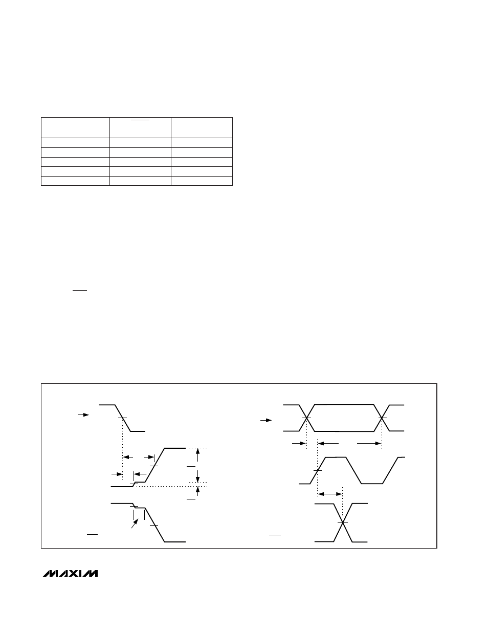
Figure 2’s timing diagram illustrates the importance of
operating the MAX555 in clocked mode. In transparent
mode (BYPASS = 1), both the master and slave registers
are transparent, and changes in input data ripple directly
to the output. Because the four MSBs are decoded into
15 identical currents, there is a decode delay for these
bits that is longer than for the eight LSBs. For the full-
scale transition case shown, an intermediate output of
1/16 full-scale occurs until the four MSBs are properly
decoded. This decode delay seriously degrades the
device’s spurious performance. In addition, skew in the
timing of the input data also directly appears at the DAC
output, further degrading high-speed performance.
MAX555 operation in the clocked mode (BYPASS = 0)
with a differential clock precludes both of these poten-
tial problems and is required for high-speed operation.
Since input data can only enter the master register
when the clock is low (while the slave register is locked
out), data-bus timing skew and the internal MSB
decode delay will not appear at the DAC output. The
DAC currents are switched only when the clock transi-
tions from low to high, after the internal data stabilizes.
Layout and Power Supplies
The MAX555 has separate pins for analog and digital
supplies. AV
EE
and DV
EE
are connected to each other
through the substrate of the IC. These potentials should
be derived from the same supply to minimize voltage
mismatch, which can cause substrate current flow and
VOUT
TRANSPARENT MODE
BYPASS = 1
CLOCKED MODE
BYPASS = 0
D0 D11
VOUT
D0 D11
CLK
VOUT
VOUT
t
SU
t
DD
F.S.
t
PD2
16
15
F.S.
16
1
t
HOLD
t
PD3
t
PD1
Figure 2. Timing Diagram
Table 1. Output Coding
100000000000
-0.499756
-0.500000
011111111111
-0.500000
-0.499756
VOUT
(V)
VOUT
(V)
000000000000
-0.999756
0
DIGITAL CODE
(D11–D0)
111111111111
0
-0.999756
000000000001
-0.999512
-0.000244