Max555 – Rainbow Electronics MAX555 User Manual
Page 6
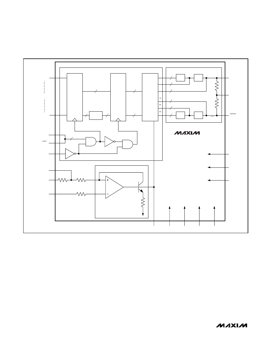
MAX555
weighted currents), which are applied directly to the out-
put of the resistor-divider network. The second group,
bits D5–D3 (three binary weighted currents), is applied
to the middle of the divider network. The middle of the
network divides the current seen at the output by 8. The
third group, bits D2–D0 (three additional binary weighted
current sources), is applied to the input of the resistive
network, dividing the current seen at the output by 64.
Glitching is reduced by decoding the four MSBs into 15
identical current sources and synchronizing data with a
master/slave register at every current switch. Data bits
are transferred to the output on the positive-going edge
of the clock, with the BYPASS input asserted low. In the
asynchronous mode with the BYPASS input asserted
high, the latches are transparent and data is trans-
ferred to the output regardless of the clock state. All
digital inputs are ECL compatible. The clock input is
differential.
The control amplifier forces a reference current, which is
replicated in the current sources. This reference current is
nominally 1.25mA. It can be supplied by an external cur-
rent source, or by an external voltage source of 1.000V
applied to the REF input.
A reference input of V
REF
= 1.000V will produce a full-
scale output voltage of V
FS
= -1.000V, where:
V
FS
= 4096 / 4095 x VOUT (code 0)
for the VOUT output. The output coding is summarized
in Table 1.
300Msps, 12-Bit DAC with
Complementary Voltage Outputs
6
_______________________________________________________________________________________
MAX555
LGND
VOUT
VOUT
50
Ω
800
Ω
800
Ω
400
Ω
400
Ω
50
Ω
I1
I2
ч 8
ч 8
IO
I3
3
4
2
15
15
8
8
I1
ч 8
ч 8
3
3
17
I2
I3
3
17
4 TO 15
DECODER
CURRENT
SOURCES
AND
SWITCHING
NETWORK
SLAVE
REGISTER
MASTER
REGISTER
12 INPUTS
DGND
AGND
AV
EE
DV
EE
LBIAS
CONTROL AMPLIFIER
I = V
IN
/R
IN
RESISTOR-DIVIDER NETWORK
MSB (D11)
CLK
CLK
BYPASS
REF/2
REF
(1V FS)
ROFFSET
LSB (D0)
ALTCOMPIB
ALTCOMPC
LOOPCRNT
AV
EE
IO
DIGITAL SECTION
Figure 1. Functional Diagram