Rainbow Electronics MAX555 User Manual
Page 2
MAX555
300Msps, 12-Bit DAC with
Complementary Voltage Outputs
2
_______________________________________________________________________________________
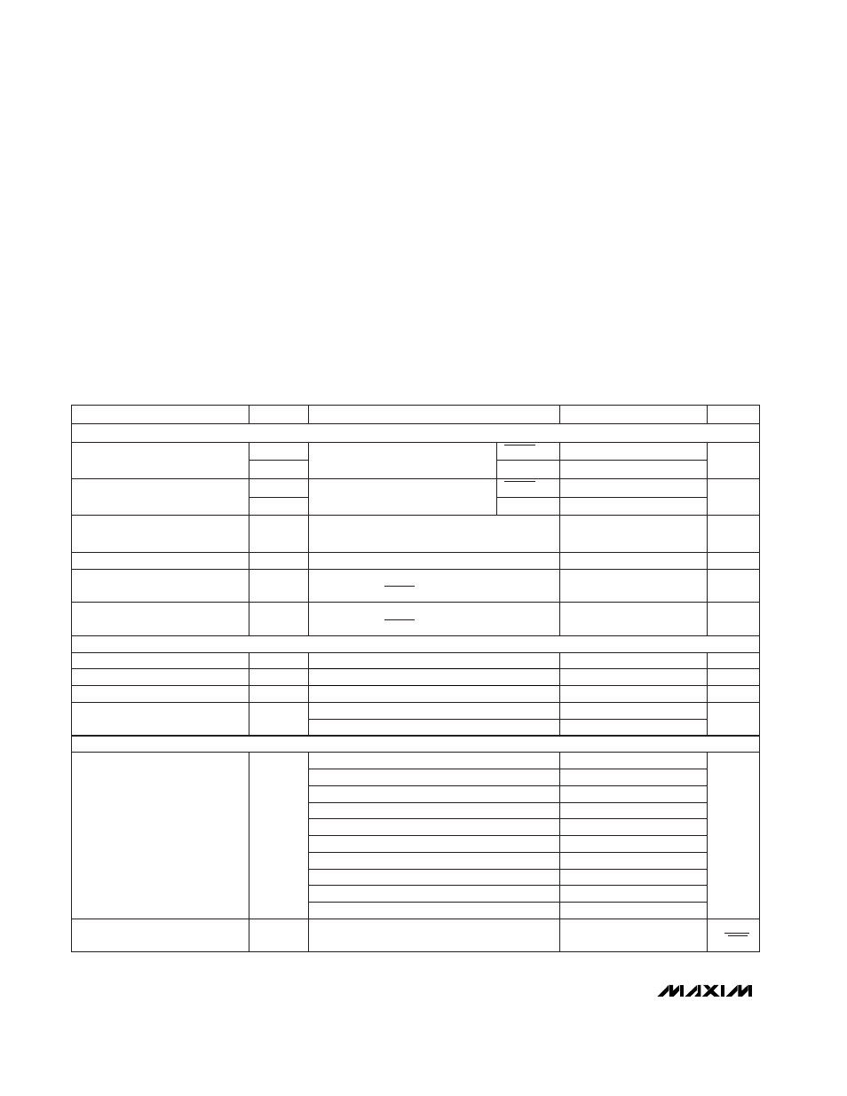
ABSOLUTE MAXIMUM RATINGS
ELECTRICAL CHARACTERISTICS
(AV
EE
= DV
EE
= -5.2V, V
REF
= 1.000V, T
MIN
to T
MAX
= 0°C to +70°C, unless otherwise noted.) (Note 2.)
Stresses beyond those listed under “Absolute Maximum Ratings” may cause permanent damage to the device. These are stress ratings only, and functional
operation of the device at these or any other conditions beyond those indicated in the operational sections of the specifications is not implied. Exposure to
absolute maximum rating conditions for extended periods may affect device reliability.
Note 1: Typical thermal resistance, junction-to-case R
θJC
= 25°C/W. See Package Information.
Analog Supply Voltage (AV
EE
) .................................-7V to +0.3V
Digital Supply Voltage (DV
EE
) ..................................-7V to +0.3V
Digital Input Voltage (D0–D11) ...................................-5.5V to 0V
Reference Input Voltage (V
IN
) .................................0V to +1.25V
Reference Input Current....................................0mA to +1.56mA
Output Compliance Voltage (V
OC
)......................-1.25V to +1.0V
Output Common-Mode Voltage (V
CM
) ................-0.25V to +1.0V
Continuous Power Dissipation (T
A
= +70°C)
(without additional heatsink) ..............................................1.3W
Operating Temperature Range...............................0°C to +70°C
Junction Temperature Range (Note 1) .................0°C to +150°C
Storage Temperature Range .............................-65°C to +150°C
Lead Temperature (soldering, 10s) .................................+300°C
V
REF
= 1.000V, current out, into
virtual ground, end-point linearity
Major carry, T
A
= +25°C
10% to 90%, T
A
= +25°C
90% to 10%, T
A
= +25°C
V
REF
= 1.000V, voltage out,
VOUT/VIN (Note 3)
±0.024% FS, 1LSB change
D0–D11 = logic 1, V
REF
= 1.000V,
measured at VOUT
±0.1% FS
CONDITIONS
ns
15
Settling Time
4
% FS
-0.05
±0.01
0.05
DLE2
Differential Linearity Error
-0.012
±0.003
0.012
DLE1
pVs
5.6
Glitch Energy
ps
570
t
RISE
Rise Time
ps
410
t
FALL
Fall Time
% FS
-1.0
±0.2
+1.0
GE
Absolute Gain Error
Guaranteed
12-Bit Monotonicity
µA
40
100
I
OS
Output Offset Current
UNITS
MIN
TYP
MAX
SYMBOL
PARAMETER
VOUT
VOUT
V
REF
= 1.000V, current out, into
virtual ground, end-point linearity
VOUT
% FS
-0.05
±0.01
0.05
ILE2
Integral Linearity Error
VOUT
-0.012
±0.006
0.012
ILE1
D0–D11 = logic 0, V
REF
= 0V,
measured at VOUT
µA
3
50
I
LEAK
Output Leakage Current
f
OUT
= 5MHz, f
CLK
= 50MHz
72
f
OUT
= 20MHz, f
CLK
= 100MHz
f
OUT
= 10MHz, f
CLK
= 50MHz
63
68
f
OUT
= 30MHz, f
CLK
= 200MHz
f
OUT
= 30MHz, f
CLK
= 100MHz
57
58
f
OUT
= 40MHz, f
CLK
= 200MHz
54
dBc
f
OUT
= 40MHz, f
CLK
= 250MHz
53
f
OUT
= 40MHz, f
CLK
= 300MHz
f
OUT
= 50MHz, f
CLK
= 250MHz
54
51
f
OUT
= 50MHz, f
CLK
= 300MHz
SFDR
Spurious-Free Dynamic Range
51
nV
√Hz
Bits 0–11 high, T
A
= +25°C
10.6
Output Noise
DC ACCURACY
TIME-DOMAIN PERFORMANCE (Note 4)
DYNAMIC PERFORMANCE (Notes 4, 5)