Electrical characteristics (continued) – Rainbow Electronics MAX555 User Manual
Page 3
MAX555
300Msps, 12-Bit DAC with
Complementary Voltage Outputs
_______________________________________________________________________________________
3
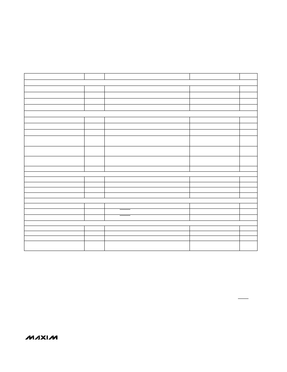
ELECTRICAL CHARACTERISTICS (continued)
(AV
EE
= DV
EE
= -5.2V, V
REF
= 1.000V, T
MIN
to T
MAX
= 0°C to +70°C, unless otherwise noted.) (Note 2.)
AV
EE
= DV
EE
= -5.2V
AV
EE
= DV
EE
= -5.2V
V
IL
= -1.95V
VOUT, VOUT
VOUT, VOUT
V
IH
= -0.75V
V
REF
= 1.000V, R
L
= 0
Ω
T
A
= +25°C
T
A
= +25°C
Bypass = 1, transparent mode (Notes 4, 7)
Bypass = 1, transparent mode (Notes 4, 7)
-3dB
V
REF
= 1.000V
Bypass = 0, clocked mode (Notes 4, 7)
Bypass = 0, clocked mode (Notes 4, 7)
Bypass = 0, clocked mode (Notes 4, 7)
Bypass = 1, transparent mode (Notes 4, 7)
CONDITIONS
mA
110
150
190
DI
EE
Digital Power-Supply Current
mA
30
46
60
AI
EE
Analog Power-Supply Current
pF
15
C
OUT
Output Capacitance
Ω
49.5
50.0
50.5
R
OUT
Output Resistance
mA
19.0
20.0
21.0
I
OUT
Full-Scale Output Current
µV
-250
0
+250
V
OS
Input Offset Voltage
kV/V
3
20
AV
OL
Open-Loop Gain
MHz
10
BW
Multiplying Input Bandwidth
Ω
775
800
825
R
IN
Amplifier Input Resistance
ps
900
t
DD
MSBs Decode Delay
µA
1
2
I
IL
Input Current, Logic Low
µA
10
200
I
IH
Input Current, Logic High
ns
2.9
t
PD1
MSBs Data-to-VOUT
Propagation Delay
ns
2
t
PD2
LSBs Data-to-VOUT
Propagation Delay
ns
2.8
t
PD3
Clock-to-VOUT
Propagation Delay
ns
0.8
t
HOLD
Data-to-Clock Hold Time
V
-1.1
-0.75
0
V
IH
Logic "1" Voltage
V
-2.0
-1.95
-1.48
V
IL
Logic "0" Voltage
ns
1
t
SU
Data-to-Clock Setup Time
UNITS
MIN
TYP
MAX
SYMBOL
PARAMETER
W
0.98
1.3
P
DISS
Power Dissipation
°C/W
25
T
JA
Package Thermal Resistance,
Junction to Ambient
Note 2: All devices are 100% production tested at +25°C and are guaranteed by design for T
A
= T
MIN
to T
MAX
as specified.
Note 3: The gain-error method of calculation is shown below:
Definition:
[V
MEASURE(FS)
- V
IDEAL(FS)
] x 100
GE(%) = ––––––––––––––––––––––––––––––––––
V
IDEAL(FS)
where FS indicates full-scale measurements.
GE Method:
GE(%) = [(4096 / 4095) V
MEASURE
- 16(V
REF
/ R
IN
) (R
OUT
)] x 100
–––––––––––––––––––––––––––––––––––––––––––––——
16(V
REF
/ R
IN
) (R
OUT
)
= [(4096 / 4095) V
MEASURE
- 1] x 100
––––––––––––––––––––––––––––––––
1
where: V
REF
= 1.000V, R
IN
= 800
Ω, R
OUT
= 50
Ω, V
MEASURE
= VOUT (FS).
Note 4: Dynamic and timing specifications are obtained from device characterization and simulation testing and are not production tested.
Note 5: Spurious-free dynamic range is measured from the fundamental frequency to any harmonic or nonharmonic spurs within the
bandwidth f
CLK
/2, unless otherwise specified.
Note 6: Guaranteed by design.
Note 7: Timing definitions are detailed in Figure 2.
Minimum data rate = DC (Note 6)
MHz
300
f
D
Data Update Rate
DIGITAL INPUTS
CONTROL AMPLIFIER
OUTPUT PERFORMANCE
POWER SUPPLIES
DIGITAL TIMING