Detailed description, Boost control scheme (pol = gnd), Inverting control scheme (pol = v – Rainbow Electronics MAX686 User Manual
Page 9
MAX686
DAC-Controlled Boost/Inverter
LCD Bias Supply with Internal Switch
_______________________________________________________________________________________
9
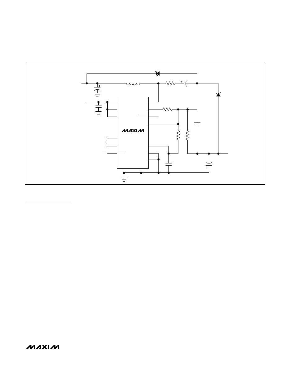
Figure 3. Alternative Negative Output Voltage Application Circuit
MAX686
V
CC
V
DD
|
V
OUT
|
≤
(27.5V - V
IN
)
D1
MBR0530L
D2
MBR0530L
L1
22
µ
H
R4
2
Ω
NEGATIVE
OUTPUT
VOLTAGE
V
IN
= 0.8V TO 27.5V
UP
POL
SHDN
DN
GND
PGND
LX
DACOUT
LCDON
FB
REF
POK
ISET
0.1
µ
F
2.2
µ
F
2.2
µ
F
R3
R2
R1
ON/OFF
DAC CONTROL
C
F
470pF
V
CC
= 2.7V TO 5.5V
0.1
µ
F
15
µ
F
Detailed Description
The MAX686 is a step-up converter that contains an
internal N-channel MOSFET switch to convert a +0.8V
to +27.5V battery voltage to a higher positive or a nega-
tive voltage. Figure 1 shows the MAX686 configured to
produce a positive output voltage. Figure 2 shows the
MAX686 configured with one additional diode and
capacitor to produce a negative output voltage. Figure
3 shows an alternative method for developing negative
output voltages. Set the output voltage with an external
resistor-divider network. Adjust the output voltage with
the internal digital-to-analog converter (DAC). The
MAX686’s current-limited pulse-frequency-modulation
(PFM) control scheme has programmable current limit-
ing and provides high efficiency over a wide range of
load conditions.
Boost Control Scheme (POL = GND)
A combination of peak current limiting and a pair of one-
shots controls the MAX686 switching. During the on-
cycle, the internal switch closes, and current through
the inductor ramps up until either the fixed 10µs maxi-
mum on-time expires (at low input voltages) or the
switch peak current limit is reached. The peak current
limit is selectable to either 500mA (ISET = V
CC
) or
250mA (ISET = GND) (see the section
Setting the Peak
Inductor Current Limit
).
After the on-cycle terminates, the switch turns off, and
the inductor charges the output capacitor through the
diode. If the output is out of regulation after the mini-
mum off-time has transpired, another on-cycle begins.
If the output is within regulation when the minimum off-
time transpires, the off-cycle extends until the output
falls out of regulation, at which point an on-cycle starts.
The MAX686 regulates the voltage on FB (V
FB
) to
1.25V. When the output is well below regulation (V
FB
is
less than 1V and the switch current limit is exceeded),
the MAX686 operates in initial power-up mode, and the
minimum off-time increases to 5µs to provide soft-start.
The switching frequency, which depends on the load,
the input voltage, and the output voltage, can be as
high as 300kHz.
Inverting Control Scheme (POL = V
CC
)
In inverting operation, the MAX686 regulates the volt-
age on FB (V
FB
) to 0V, and the error amplifier’s polarity
is reversed. The minimum off-time changes to 3.5µs for
negative output voltages. When the output is well below
regulation (V
FB
is 0.25V or more and the switch current
limit is exceeded), initial power-up is assumed, and the
minimum off-time increases to 5µs to provide soft-start.