Electrical characteristics – Rainbow Electronics MAX686 User Manual
Page 4
MAX686
DAC-Controlled Boost/Inverter
LCD Bias Supply with Internal Switch
4
_______________________________________________________________________________________
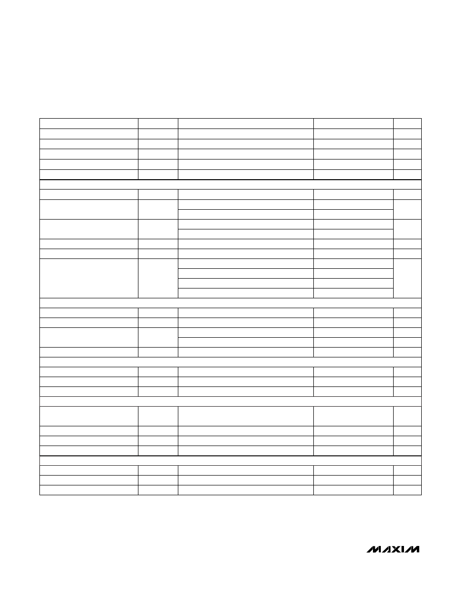
ISET = V
CC
A
0.4
0.6
SHDN = GND
I
LX
LX Switch Current Limit
POL = GND, VFB = 1.3V, I
DACOUT
= 0mA
ISET = GND
V
CC
= V
DD
= 5V, I
LX
= 100mA
0.2
0.3
Ω
1.2
V
LX
= 28V
Rising or falling
µA
1.5
CONDITIONS
I
LXLEAK
LX Leakage Current
R
LX
LX On-Resistance
V
CC
= V
DD
= 3.3V, I
LX
= 100mA
1.6
µs
7.5
12.5
t
ON
Maximum LX On-Time
POL = GND, V
FB
> 1.2V
µs
0.7
1.3
t
OFF
Minimum LX Off-Time
POL = V
CC
, V
FB
< 0.15V
2.8
4.2
POL = GND, V
FB
< 0.8V
3.8
6.2
POL = V
CC
, V
FB
> 0.4V
3.8
6.2
µA
4
I
SHDN
Shutdown Current
µA
125
I
CC
+ I
DD
V
2.7
5.5
V
CC
, V
DD
Supply Voltage (Note 1)
Supply Current
V
28
V
LX
LX Voltage Range
V
2.10
2.65
V
LOCK
V
CC
Undervoltage Lockout
UNITS
MIN
TYP
MAX
SYMBOL
PARAMETER
ELECTRICAL CHARACTERISTICS
(V
CC
= V
DD
= V
IN
= +5V, C
REF
= 0.1µF,
T
A
= -40°C to +85°C
, unless otherwise noted.) (Note 4)
Note 1:
The MAX686 requires a supply voltage at V
CC
= V
DD
between +2.7V and +5.5V; however, the voltage that supplies the
inductor can vary from +0.8V to +27.5V, depending on circuit operating conditions.
Note 2:
The DAC output is set to its midpoint value at power-on.
Note 3:
The DAC setting is guaranteed to remain valid as long as V
CC
is greater than the V
CC
DAC Reset Threshold.
Note 4:
Specifications to -40°C are guaranteed by design, not production tested.
V
CC
= V
DD
= 2.7V to 5.5V, no load
V
1.22
1.28
V
REF
REF Output Voltage
I
REF
= 0µA to 25µA, C
REF
= 0.1µF
mV
10
REF Load Regulation
POL = GND
V
1.22
1.28
V
FB
FB Set Point
POL = V
CC
-15
15
nA
±50
I
FB
FB Input Bias Current
V
POK
rising
V
1.05
1.20
V
POK
POK Threshold
nA
±50
I
POK
POK Input Current
V
LCDON
= 0.4V, V
POK
= 1.25V
mA
2
I
LCDON
LCDON Sink Current
mV
Voltage applied to L1
V
0.8
V
OUT
V
IN
Input Voltage
-50µA < I
DACOUT
< 0µA
V
V
REF
-
V
REF
+
0.02
0.02
V
FS
Full-Scale Output Voltage
0µA < I
DACOUT
< 20µA
mV
0
15
V
ZS
Zero-Scale Output Voltage
Bits
6
Resolution
Mid-scale = V
REF
x 32/63
%
-3
3
MSA
Mid-Scale Accuracy
2.7V < V
CC
= V
DD
< 5.5V
V
0.7
V
IL
Input Low Level
2.7V < V
CC
= V
DD
< 5.5V
V
2.4
V
IH
Input High Level
µA
±1
I
BIAS
Input Bias Current
LX
REFERENCE AND FB INPUT
POWER OK COMPARATOR,
LCDON
OUTPUT
LOGIC INPUTS: POL, ISET, UP, DN
,
SHDN
DAC OUTPUT
(Notes 2, 3)