Rainbow Electronics MAX686 User Manual
Page 2
MAX686
DAC-Controlled Boost/Inverter
LCD Bias Supply with Internal Switch
2
_______________________________________________________________________________________
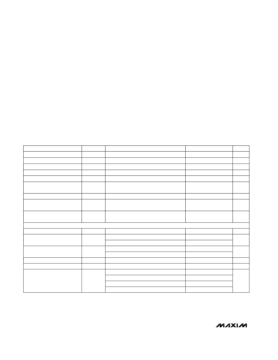
ABSOLUTE MAXIMUM RATINGS
ELECTRICAL CHARACTERISTICS
(V
CC
= V
DD
= V
IN
= +5V, C
REF
= 0.1µF,
T
A
= 0°C to +85°C,
unless otherwise noted. Typical values are at T
A
= +25°C.)
Stresses beyond those listed under “Absolute Maximum Ratings” may cause permanent damage to the device. These are stress ratings only, and functional
operation of the device at these or any other conditions beyond those indicated in the operational sections of the specifications is not implied. Exposure to
absolute maximum rating conditions for extended periods may affect device reliability.
Voltage
V
CC
, ISET, POK, POL, SHDN,
UP, DN, V
DD
to GND ...........................................-0.3V to +6V
FB, REF, DACOUT to GND.......................-0.3V to (V
CC
+ 0.3V)
PGND to GND .....................................................-0.3V to +0.3V
LX, LCDON to GND..............................................-0.3V to +30V
Current
LX (sinking) .....................................................................600mA
LCDON (sinking)...............................................................10mA
Continuous Power Dissipation (T
A
= +70°C)
QSOP (derate 8.30mW/°C above +70°C) ......................667mW
Operating Temperature Ranges
MAX686C/D ..........................................................0°C to +70°C
MAX686EEE.......................................................-40°C to +85°C
Storage Temperature Range .............................-65°C to +160°C
Lead Temperature (soldering, 10sec) .............................+300°C
SHDN = GND
POL = GND, V
FB
= 1.3V, I
DACOUT
= 0mA
Boost configuration, V
OUT
= 27.5V,
I
LOAD
= 0mA to 5mA
Boost configuration, V
OUT
= 27.5V,
I
LOAD
= 5mA, V
CC
= V
DD
= 2.7V to 5.5V
Rising or falling
CONDITIONS
µA
1.3
4
I
SHDN
Shutdown Current
µA
65
125
I
CC
+ I
DD
V
2.7
5.5
V
CC
, V
DD
Supply Voltage (Note 1)
Supply Current
V
28
V
LX
LX Voltage Range
%/mA
0.01
Load Regulation
%/V
0.1
Line Regulation
V
2.10
2.5
2.65
V
LOCK
V
CC
Undervoltage Lockout
mV
100
V
CC
Undervoltage Lockout
Hysteresis
V
0.5
1.5
2.1
V
RESET
V
CC
DAC Reset Threshold
UNITS
MIN
TYP
MAX
SYMBOL
PARAMETER
ISET = V
CC
A
0.42
0.50
0.58
I
LX
LX Switch Current Limit
ISET = GND
0.21
0.25
0.29
V
LX
= 28V
µA
1.5
I
LXLEAK
LX Leakage Current
V
CC
= V
DD
= 5V, I
LX
= 100mA
Ω
0.6
1.2
R
LX
LX On-Resistance
V
CC
= V
DD
= 3.3V, I
LX
= 100mA
0.8
1.6
µs
8
10
12
t
ON
Maximum LX On-Time
POL = GND, V
FB
> 1.2V
µs
0.8
1
1.2
t
OFF
Minimum LX Off-Time
POL = V
CC
, V
FB
< 0.15V
2.8
3.5
4.2
POL = GND, V
FB
< 0.8V
4
5
6
POL = V
CC
, V
FB
> 0.4V
4
5
6
Voltage applied to L1
V
0.8
V
OUT
V
IN
Input Voltage
LX