Table 2. conversion register – Rainbow Electronics MAX1031 User Manual
Page 13
MAX1027/MAX1029/MAX1031
10-Bit 300ksps ADCs with FIFO,
Temp Sensor, Internal Reference
______________________________________________________________________________________
13
pair and one of them has been reconfigured as CNVST
or REF-, the pair is ignored.
Select scan mode 00 or 01 to return one result per sin-
gle-ended channel and one result per differential pair
within the requested range, plus one temperature result
if selected. Select scan mode 10 to scan a single input
channel numerous times, depending on NSCAN1 and
NSCAN0 in the averaging register (see Table 6). Select
scan mode 11 to return only one result from a single
channel.
Setup Register
Write a byte to the setup register to configure the clock,
reference, and power-down modes. Table 3 details the
bits in the setup register. Bits 5 and 4 (CKSEL1 and
CKSEL0) control the clock mode, acquisition and sam-
pling, and the conversion start. Bits 3 and 2 (REFSEL1
and REFSEL0) control internal or external reference use.
Bits 1 and 0 (DIFFSEL1 and DIFFSEL0) address the
unipolar mode and bipolar mode registers and configure
the analog input channels for differential operation.
Unipolar/Bipolar Registers
The final 2 bits (LSBs) of the setup register control the
unipolar/bipolar mode address registers. Set bits 1 and
0 (DIFFSEL1 and DIFFSEL0) to 10 to write to the unipo-
lar mode register. Set bits 1 and 0 to 11 to write to the
bipolar mode register. In both cases, the setup byte
must be followed immediately by 1 byte of data written
to the unipolar register or bipolar register. Hold CS low
and run 16 SCLK cycles before pulling CS high. If the
last 2 bits of the setup register are 00 or 01, neither the
unipolar mode register nor the bipolar mode register is
written. Any subsequent byte is recognized as a new
input data byte. See Tables 4 and 5 to program the
unipolar and bipolar mode registers.
If a channel is configured as both unipolar and bipolar,
the unipolar setting takes precedence. In unipolar
mode, AIN+ can exceed AIN- by up to V
REF
. The out-
put format in unipolar mode is binary. In bipolar mode,
either input can exceed the other by up to V
REF
/ 2. The
output format in bipolar mode is two's complement.
Averaging Register
Write to the averaging register to configure the ADC to
average up to 32 samples for each requested result,
and to independently control the number of results
requested for single-channel scans.
Table 2 details the four scan modes available in the con-
version register. All four scan modes allow averaging as
long as the AVGON bit, bit 4 in the averaging register, is
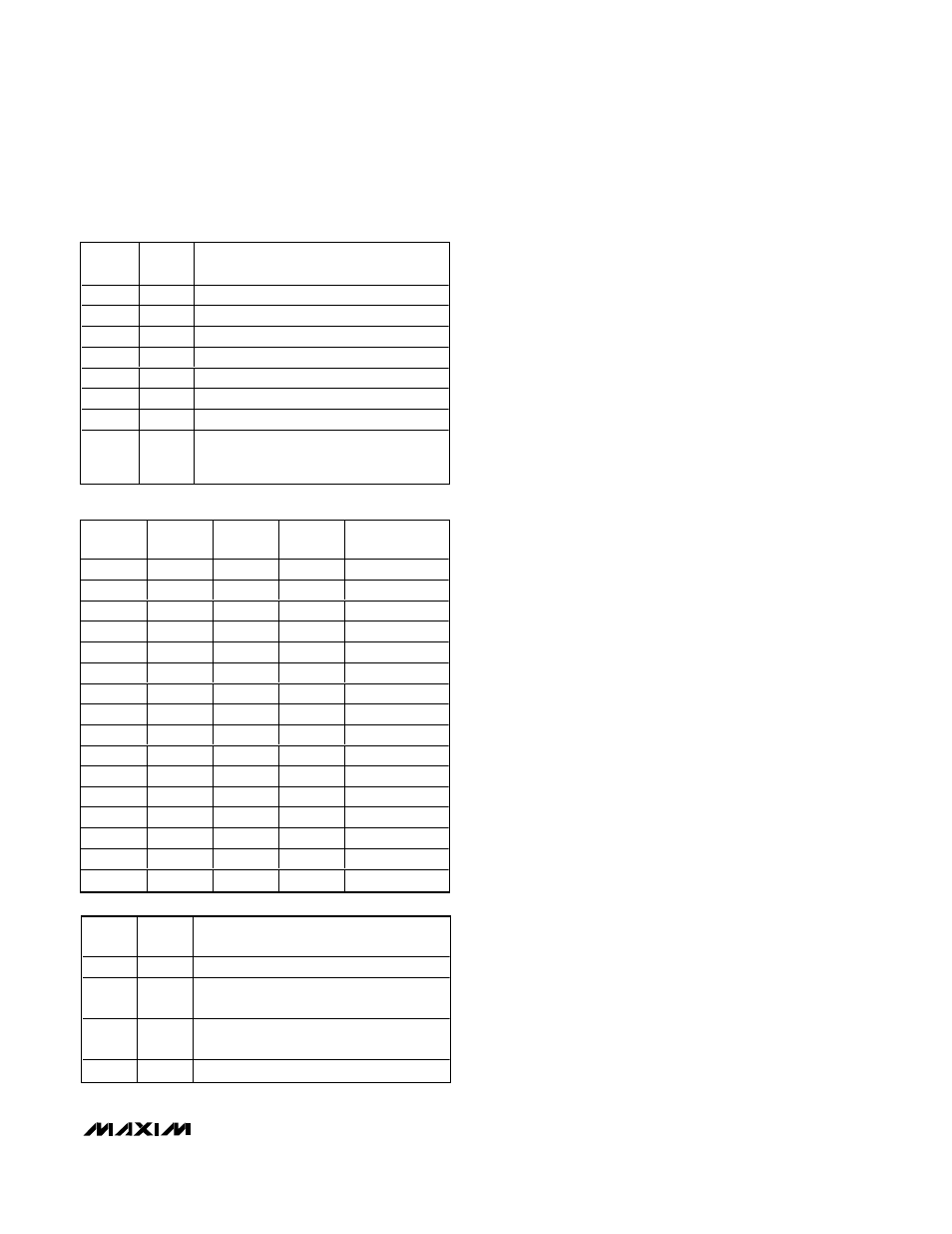
BIT
NAME
BIT
FUNCTION
—
7 (MSB) Set to 1 to select conversion register.
CHSEL3
6
Analog input channel select.
CHSEL2
5
Analog input channel select.
CHSEL1
4
Analog input channel select.
CHSEL0
3
Analog input channel select.
SCAN1
2
Scan mode select.
SCAN0
1
Scan mode select.
TEMP
0 (LSB)
Set to 1 to take a single temperature
measurement. The first conversion result
of a scan contains temperature information.
Table 2. Conversion Register*
*See below for bit details.
CHSEL3
CHSEL2
CHSEL1
CHSEL0
SELECTED
CHANNEL (N)
0
0
0
0
AIN0
0
0
0
1
AIN1
0
0
1
0
AIN2
0
0
1
1
AIN3
0
1
0
0
AIN4
0
1
0
1
AIN5
0
1
1
0
AIN6
0
1
1
1
AIN7
1
0
0
0
AIN8
1
0
0
1
AIN9
1
0
1
0
AIN10
1
0
1
1
AIN11
1
1
0
0
AIN12
1
1
0
1
AIN13
1
1
1
0
AIN14
1
1
1
1
AIN15
SCAN1 SCAN0
SCAN MODE (CHANNEL N IS
SELECTED BY BITS CHSEL3–CHSEL0)
0
0
Scans channels 0 through N.
0
1
Scans channels N through the highest
numbered channel.
1
0
S cans channel N r ep eated l y. The aver ag i ng
r eg i ster sets the num b er of r esul ts.
1
1
No scan. Converts channel N once only.