Detailed description, Pin description – Rainbow Electronics MAX1089 User Manual
Page 7
MAX1086–MAX1089
150ksps, 10-Bit, 2-Channel Single-Ended, and
1-Channel True-Differential ADCs in SOT23
_______________________________________________________________________________________
7
Detailed Description
The MAX1086–MAX1089 analog-to-digital converters
(ADCs) use a successive-approximation conversion
(SAR) technique and an on-chip track-and-hold (T/H)
structure to convert an analog signal into a 10-bit digital
result.
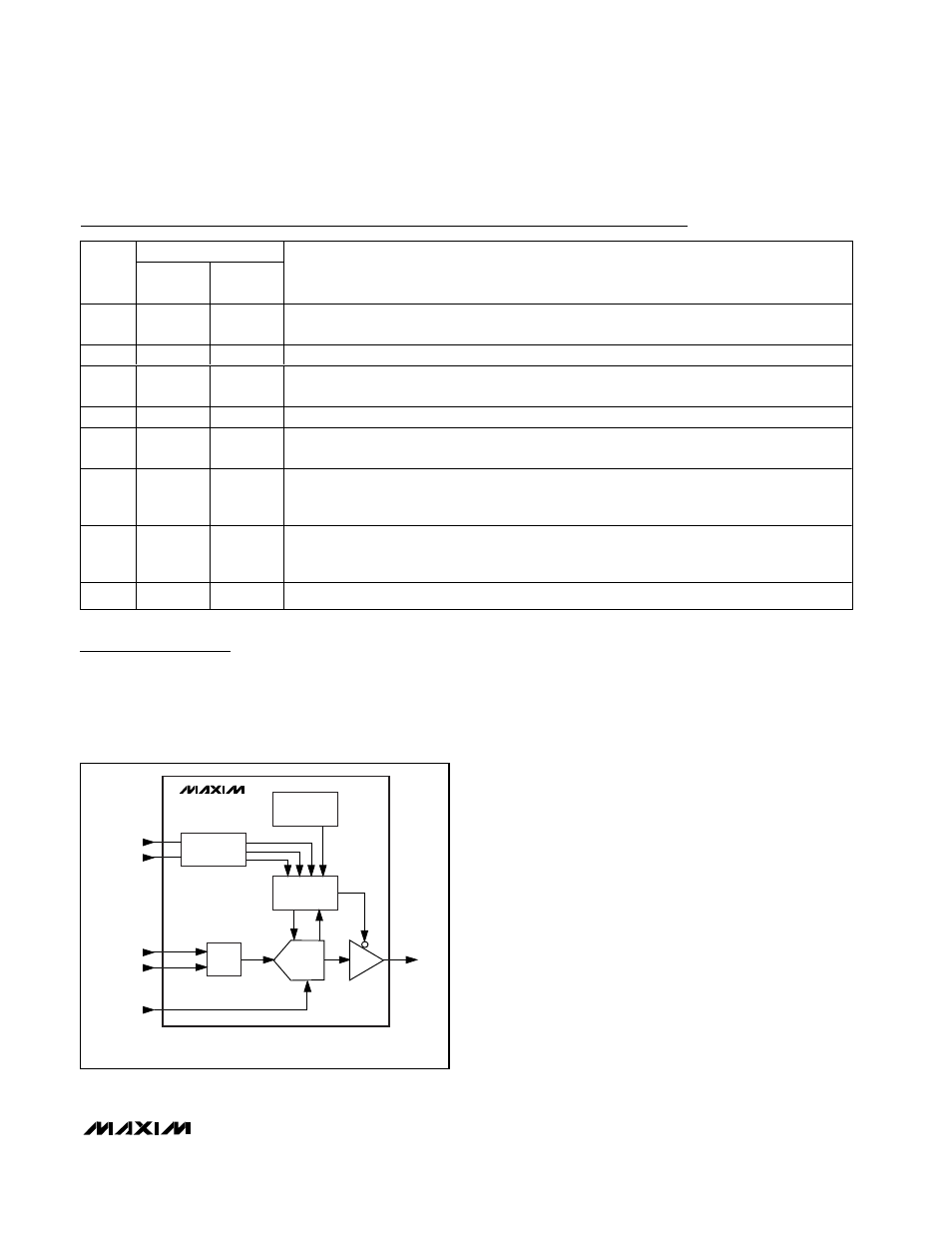
The serial interface provides easy interfacing to micro-
processors (µPs). Figure 3 shows the simplified internal
structure for the MAX1086/MAX1087 (2–channels, sin-
gle-ended) and the MAX1088/MAX1089 (1–channel,
true-differential).
True-Differential Analog Input Track/Hold
The equivalent circuit of Figure 4 shows the
MAX1086–MAX1089’s input architecture which is com-
posed of a T/H, input multiplexer, comparator, and
switched-capacitor DAC. The T/H enters its tracking
mode on the rising edge of CNVST. The positive input
capacitor is connected to AIN1 or AIN2 (MAX1086/
MAX1087) or AIN+ (MAX1088/MAX1089). The negative
input capacitor is connected to GND (MAX1086/
MAX1087) or AIN- (MAX1088/MAX1089). The T/H
enters its hold mode on the falling edge of CNVST and
the difference between the sampled positive and nega-
tive input voltages is converted. The time required for
the T/H to acquire an input signal is determined by how
quickly its input capacitance is charged. If the input
signal’s source impedance is high, the acquisition time
lengthens, and CNVST must be held high for a longer
period of time. The acquisition time, t
ACQ
, is the maxi-
mum time needed for the signal to be acquired, plus
the power-up time. It is calculated by the following
equation:
t
ACQ
= 7 x (R
S
+ R
IN
) x 24pF + t
PWR
Pin Description
NAME
PIN
MAX1086
MAX1087
MAX1088
MAX1089
FUNCTION
1
V
DD
V
DD
Positive Supply Voltage. +2.7V to +3.6V (MAX1087/MAX1089); +4.75V to +5.25V
(MAX1086/MAX1088). Bypass with a 0.1µF capacitor to GND.
2
AIN1
AIN+
Analog Input Channel 1 (MAX1086/MAX1087) or Positive Analog Input (MAX1088/MAX1089)
3
AIN2
AIN-
Analog Input Channel 2 (MAX1086/MAX1087) or Negative Analog Input (MAX1088/MAX1089)
4
GND
GND
Ground
5
REF
REF
External Reference Voltage Input. Sets the analog voltage range. Bypass with a 0.1µF
capacitor to GND.
6
CNVST
CNVST
Conversion Start. A rising edge powers-up the IC and places it in track mode. At the falling
edge of CNVST, the device enters hold mode and begins conversion. CNVST also selects the
input channel (MAX1086/MAX1087) or input polarity (MAX1088/MAX1089).
7
DOUT
DOUT
Serial Data Output. DOUT transitions the falling edge of SCLK. DOUT goes low at the start of a
conversion and presents the MSB at the completion of a conversion. DOUT goes high-
impedance once data has been fully clocked out.
8
SCLK
SCLK
Serial Clock Input. Clocks out data at DOUT MSB first.
10-BIT
SAR
ADC
CONTROL
OSCILLATOR
INPUT SHIFT
REGISTER
T/H
REF
CNVST
SCLK
DOUT
AIN2
(AIN-)
AIN1
(AIN+)
MAX1086–MAX1089
( ) ARE FOR MAX1088/MAX1089
Figure 3. Simplified Functional Diagram