Applications information, Transfer function – Rainbow Electronics MAX1089 User Manual
Page 10
MAX1086–MAX1089
150ksps, 10-Bit, 2-Channel Single-Ended, and
1-Channel True-Differential ADCs in SOT23
10
______________________________________________________________________________________
Output Data Format
Figures 5a and 5b illustrate the conversion timing for
the MAX1086–MAX1089. The 10-bit conversion result is
output in MSB first format, followed by two sub-bits (S1
and S0). Data on DOUT transitions on the falling edge
of SCLK. All 12-bits must be clocked out before CNVST
transitions again. For the MAX1088/MAX1089, data is
straight binary for unipolar mode and two’s comple-
ment for bipolar mode. For the MAX1086/MAX1087,
data is always straight binary.
Applications Information
Automatic Shutdown Mode
With CNVST low, the MAX1086–MAX1089 defaults to an
AutoShutdown state (<0.2µA) after power-up and
between conversions. After detecting a rising edge on
CNVST, the part powers up, sets DOUT low and enters
track mode. After detecting a falling-edge on CNVST, the
device enters hold mode and begins the conversion. A
maximum of 3.7µs later, the device completes conver-
sion, enters shutdown and MSB is available at DOUT.
External Reference
An external reference is required for the MAX1086–
MAX1089. Use a 0.1µF bypass capacitor for best per-
formance. The reference input structure allows a volt-
age range of +1V to V
DD
+ 50mV.
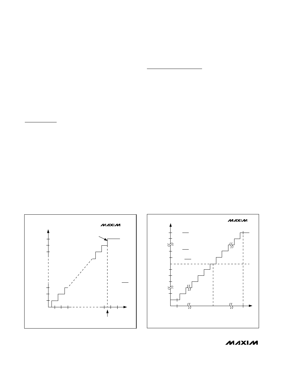
Transfer Function
Figure 6 shows the unipolar transfer function for the
MAX1086–MAX1089. Figure 7 shows the bipolar transfer
function for the MAX1088/MAX1089. Code transitions
occur halfway between successive-integer LSB values.
Connection to Standard Interfaces
The MAX1086–MAX1089 feature a serial interface that is
fully compatible with SPI, QSPI, and MICROWIRE. If a
serial interface is available, establish the CPU’s serial
interface as a master, so that the CPU generates the seri-
al clock for the ADCs. Select a clock frequency up to
8MHz.
How to Perform a Conversion
1)
Use a general purpose I/O line on the CPU to hold
CNVST low between conversions.
2)
Drive CNVST high to acquire AIN1(MAX1086/
MAX1087) or unipolar mode (MAX1088/MAX1089).
To acquire AIN2(MAX1086/MAX1087) or bipolar
mode (MAX1088/MAX1089), drive CNVST low and
high again.
3)
Hold CNVST high for 1.4µs.
4)
Drive CNVST low and wait approximately 3.7µs for
conversion to complete. After 3.7µs, the MSB is
available at DOUT.
5)
Activate SCLK for a minimum of 12 rising clock
edges. DOUT transitions on SCLK’s falling edge
OUTPUT CODE
FULL-SCALE
TRANSITION
11 . . . 111
11 . . . 110
11 . . . 101
00 . . . 011
00 . . . 010
00 . . . 001
00 . . . 000
1
2
3
0
FS
FS - 3/2LSB
FS = V
REF
ZS = GND
INPUT VOLTAGE (LSB)
1LSB =
V
REF
1024
MAX1086–
MAX1089
Figure 6. Unipolar Transfer Function
011 . . . 111
011 . . . 110
000 . . . 010
000 . . . 001
000 . . . 000
111 . . . 111
111 . . . 110
111 . . . 101
100 . . . 001
100 . . . 000
- FS
0
INPUT VOLTAGE (LSB)
OUTPUT CODE
ZS = 0
+FS - 1LSB
*V
COM
V
REF
/ 2 *V
IN
= (AIN+) - (AIN-)
FS
=
V
REF
2
-FS =
-V
REF
2
1LSB =
V
REF
1024
≤
MAX1088/MAX1089
Figure 7. Bipolar Transfer Function