Timing characteristics (figures 1 and 2) – Rainbow Electronics MAX1089 User Manual
Page 4

MAX1086–MAX1089
150ksps, 10-Bit, 2-Channel Single-Ended, and
1-Channel True-Differential ADCs in SOT23
4
_______________________________________________________________________________________
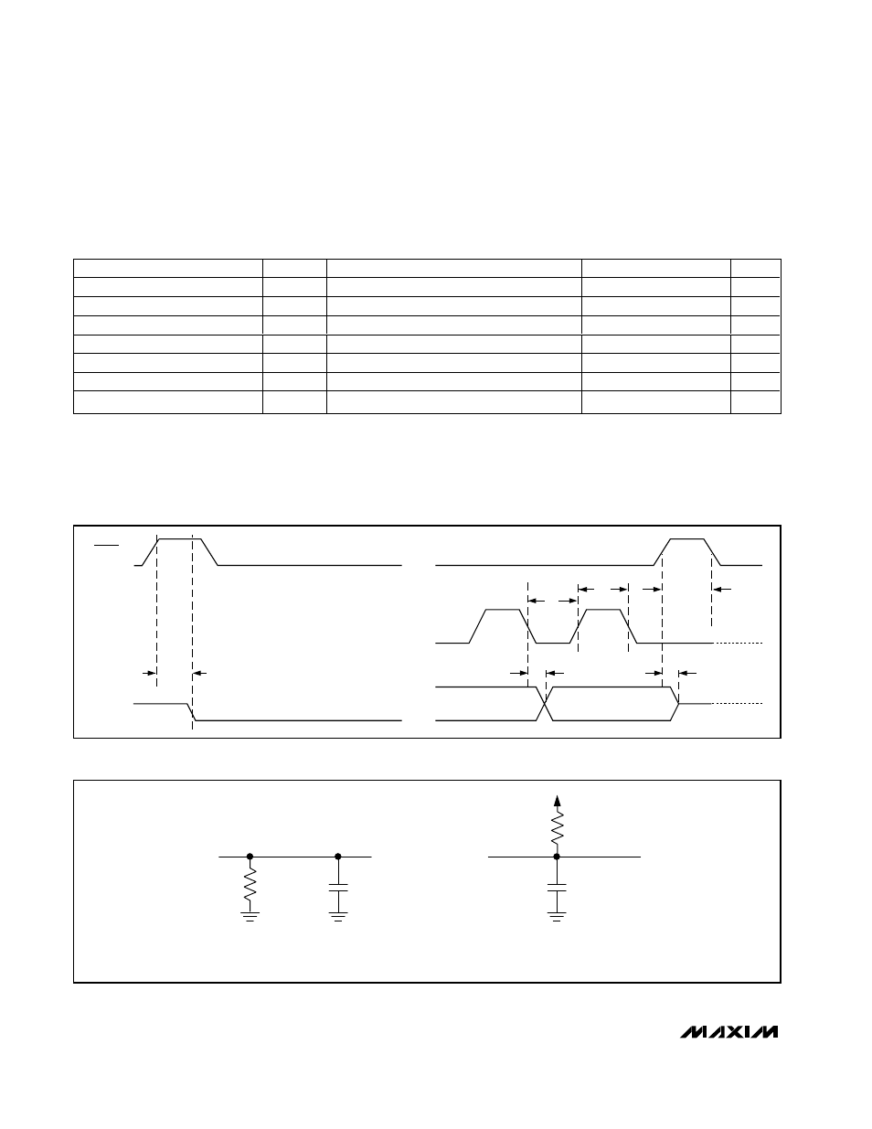
TIMING CHARACTERISTICS (Figures 1 and 2)
(V
DD
= +2.7V to +3.6V, V
REF
= +2.5V for MAX1087/MAX1089, or V
DD
= +4.75V to +5.25V, V
REF
= +4.096V for MAX1086/MAX1088,
0.1µF capacitor at REF, f
SCLK
= 8MHz (50% duty cycle); AIN- = GND for MAX1088/MAX1089. T
A
= T
MIN
to T
MAX,
unless otherwise
noted. Typical values at T
A
= +25°C.)
PARAMETERS
SYMBOL
CONDITIONS
MIN
TYP
MAX
UNITS
SCLK Pulse Width High
t
CH
38
ns
SCLK Pulse Width Low
t
CL
38
ns
SCLK Fall to DOUT Transition
t
DOT
C
LOAD
= 30pF
60
ns
SCLK Rise to DOUT Disable
t
DOD
C
LOAD
= 30pF
100
500
ns
CNVST Rise to DOUT Enable
t
DOE
C
LOAD
= 30pF
80
ns
CNVST Fall to MSB Valid
t
DOV
C
LOAD
= 30pF
3.7
µs
CNVST Pulse Width
t
CSW
30
ns
Note 1: Unipolar input.
Note 2: Relative accuracy is the deviation of the analog value at any code from its theoretical value after offset and gain errors have
been removed.
Note 3: Offset nulled.
Note 4: The absolute input range for the analog inputs is from GND to V
DD
.
• • •
• • •
• • •
CNVST
SCLK
DOUT
t
DOE
HIGH-Z
HIGH-Z
t
CSW
t
DOT
t
CL
t
CH
t
DOD
DOUT
6k
Ω
6k
Ω
C
L
GND
DOUT
C
L
GND
V
DD
a) HIGH -Z TO V
OH
, V
OL
TO V
OH
, AND V
OH
TO HIGH -Z
a) HIGH -Z TO V
OL
, V
OH
TO V
OL
, AND V
OL
TO HIGH -Z
Figure 1. Detailed Serial-Interface Timing Sequence
Figure 2. Load Circuits for Enable/Disable Times
