Ac electrical characteristics—vga mode – Rainbow Electronics MAX2038 User Manual
Page 4
MAX2038
Ultrasound VGA Integrated
with CW Octal Mixer
4
_______________________________________________________________________________________
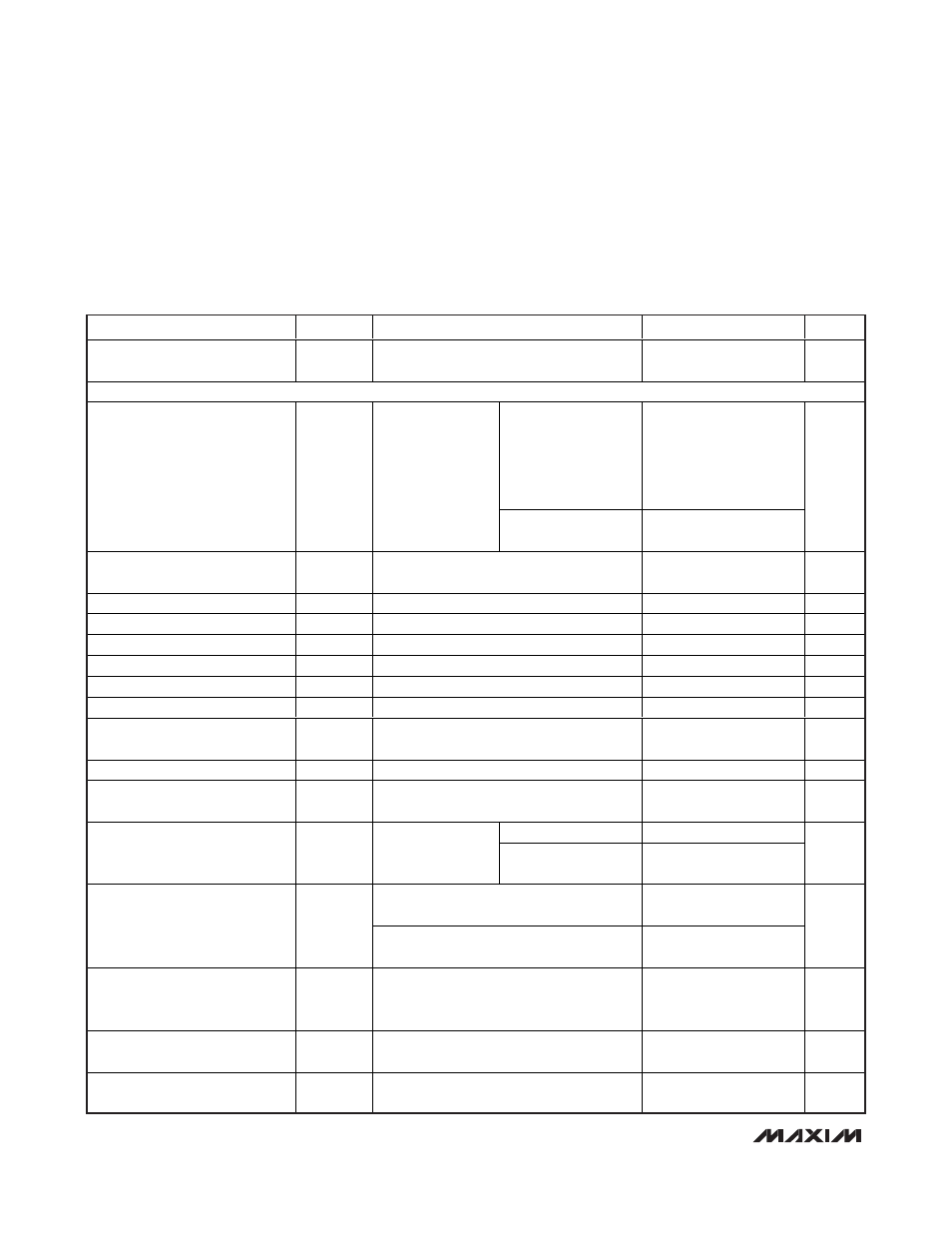
AC ELECTRICAL CHARACTERISTICS—VGA MODE
(
Typical Application Circuit, Figure 7. V
CC
= V
REF
= 4.75V to 5.25V, V
CM
= (3/5)V
REF
, T
A
= 0
°C to +70°C, V
GND
= 0, LOW_PWR = 0,
M4_EN = 0, CW_FILTER = 1, TMODE = 0, PD = 0, CW_VG = 1, CW_M1 = 0, CW_M2 = 0, VG_CLAMP_MODE = 1, f
RF
= f
LO
/16 =
5MHz, capacitance to GND at each of the VGA differential outputs is 60pF, differential capacitance across the VGA outputs is 10pF,
R
L
= 1k
Ω, CW mixer outputs pulled up to +11V through four separate ±0.1% 115Ω resistors, differential mixer inputs are driven from
a low impedance source. Typical values are at V
CC
= V
REF
= 5V, T
A
= +25
°C, unless otherwise noted.) (Note 2)
PARAMETER
SYMBOL
CONDITIONS
MIN
TYP
MAX
UNITS
Mode Select Response Time
CW_VG set from logic 1 to 0 or from 0 to 1
(Note 9)
2
µs
VGA MODE
Differential output
capacitance is 10pF,
capacitance to GND
at each single-ended
output is 60pF,
R
L
= 1k
Ω
18
Full-Scale Bandwidth
f-1.3dB
V
OUT
= 1.5V
P-P
,
1.3dB bandwidth,
gain = 10dB
No capacitive load
R
L
= 1k
Ω
29
MHz
Small-Signal Bandwidth
f-1.3dB
V
OUT
= 1.5mV
P-P
, 3dB bandwidth,
gain = 10dB
30
MHz
Differential Input Resistance
R
IN
170
200
230
Ω
Input Effective Capacitance
C
IN
f
RF
= 10MHz, each input to ground
15
pF
Differential Output Resistance
R
OUT
100
Ω
Maximum Gain
+29.5
dB
Minimum Gain
-12.5
dB
Gain Range
42
dB
Absolute Gain Error
T
A
= +25
°C, full gain range 0% to 100%,
V
REF
= 5V
±0.25
±1.5
dB
VGA Gain Response Time
40dB gain change to within 1dB final value
1
µs
Input-Referred Noise
VG_CTL set for maximum gain,
no input signal
2
nV/
√Hz
No input signal
22
Output-Referred Noise
VG_CTL set for
+10dB of gain
V
OUT
= 1.5V
P-P
, 1kHz
offset
55
nV/
√Hz
V G_C LAM P _M OD E = 1, V G_C TL set for
+ 10d B of g ai n, f
R F
= 5M H z, V
OU T
= 1.5V
P - P
-70
Second Harmonic
HD2
V G_C LAM P _M OD E = 1, V G _C TL set for
+ 10d B of g ai n, f
R F
= 10M H z, V
OU T
= 1.5V
P - P
-55
-65
dBc
Third-Order Intermodulation
Distortion
IMD3
V G_C LT set for + 10d B of g ai n, f
RF1
= 5M H z,
f
R F2
= 5.01MHz, V
OUT
= 1.5V
P-P
,
V
REF
= 5V (Note 3)
-40
-52
dBc
Channel-to-Channel Crosstalk
V
OUT
= 1V
P-P
differential, f
R F
= 10MHz,
VG_CTL set for +10dB of gain
-80
dB
Maximum Output Voltage at
ClampON
VG_CLAMP_MODE = 0, VG_CTL set for
+20dB of gain, 350mV
P-P
differential input
2.4
V
P-P
d i ffer enti al