Pin description – Rainbow Electronics MAX2057 User Manual
Page 9
MAX2057
1700MHz to 2500MHz Variable-Gain
Amplifier with Analog Gain Control
_______________________________________________________________________________________
9
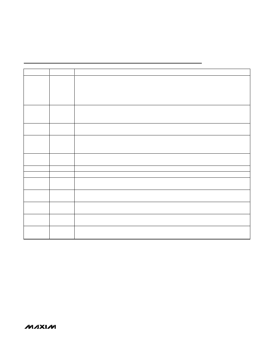
Pin Description
PIN
NAME
FUNCTION
1, 3, 4, 6, 7,
9, 10, 12, 14,
18, 19,
21–24, 27,
28, 30, 31,
33, 34, 36
GND
Ground. Connect to the board’s ground plane using low-inductance layout techniques.
2
OUT_A
Second-Attenuator Output. Internally matched to 50
Ω over the operating frequency band. Connect to
IN through a DC-blocking capacitor if greater than 21dB of gain-control range is required. No
connection is required if the second attenuator is not used.
5, 13, 16, 25,
32
V
CC
Power Supply. Bypass each pin to GND with capacitors as shown in the Typical Application Circuit.
Place capacitors as close to the pin as possible.
8
IN_A
Second-Attenuator Input. Internally matched to 50
Ω over the operating frequency band. Connect to a
50
Ω RF source through a DC-blocking capacitor if greater than 21dB of gain-control range is
required. No connection is required if the second attenuator is not used.
11
V
CNTL
Analog Gain-Control Input. Limit voltages applied to this pin to a 1V to 4.5V range when V
CC
is
present to ensure device reliability.
15
R
SET1
First-Stage Amplifier Bias-Current Setting. Connect to GND through a 1.2k
Ω resistor.
17
R
SET2
Second-Stage Amplifier Bias-Current Setting. Connect to GND through a 2k
Ω resistor.
20
OUT
RF Output. Internally matched to 50
Ω over the operating frequency band. Requires a DC-blocking
capacitor and a shunt-matching capacitor.
26
AMP_IN
Amplifier Input. Internally matched to 50
Ω over the operating frequency band. Connect to ATTN_OUT
through a DC-blocking capacitor.
29
ATTN_OUT
Attenuator Output. Internally matched to 50
Ω over the operating frequency band. Connect to AMP_IN
through a DC-blocking capacitor.
35
IN
RF Input. Internally matched to 50
Ω over the operating frequency band. Connect to a 50Ω RF source
through a DC-blocking capacitor if the second attenuator is not used.
Exposed
Paddle
GND
Exposed Paddle Ground Plane. This paddle affects RF performance and provides heat dissipation.
This paddle MUST be soldered evenly to the board’s ground plane for proper operation.