Ac electrical characteristics (continued) – Rainbow Electronics MAX2057 User Manual
Page 3
MAX2057
1700MHz to 2500MHz Variable-Gain
Amplifier with Analog Gain Control
_______________________________________________________________________________________
3
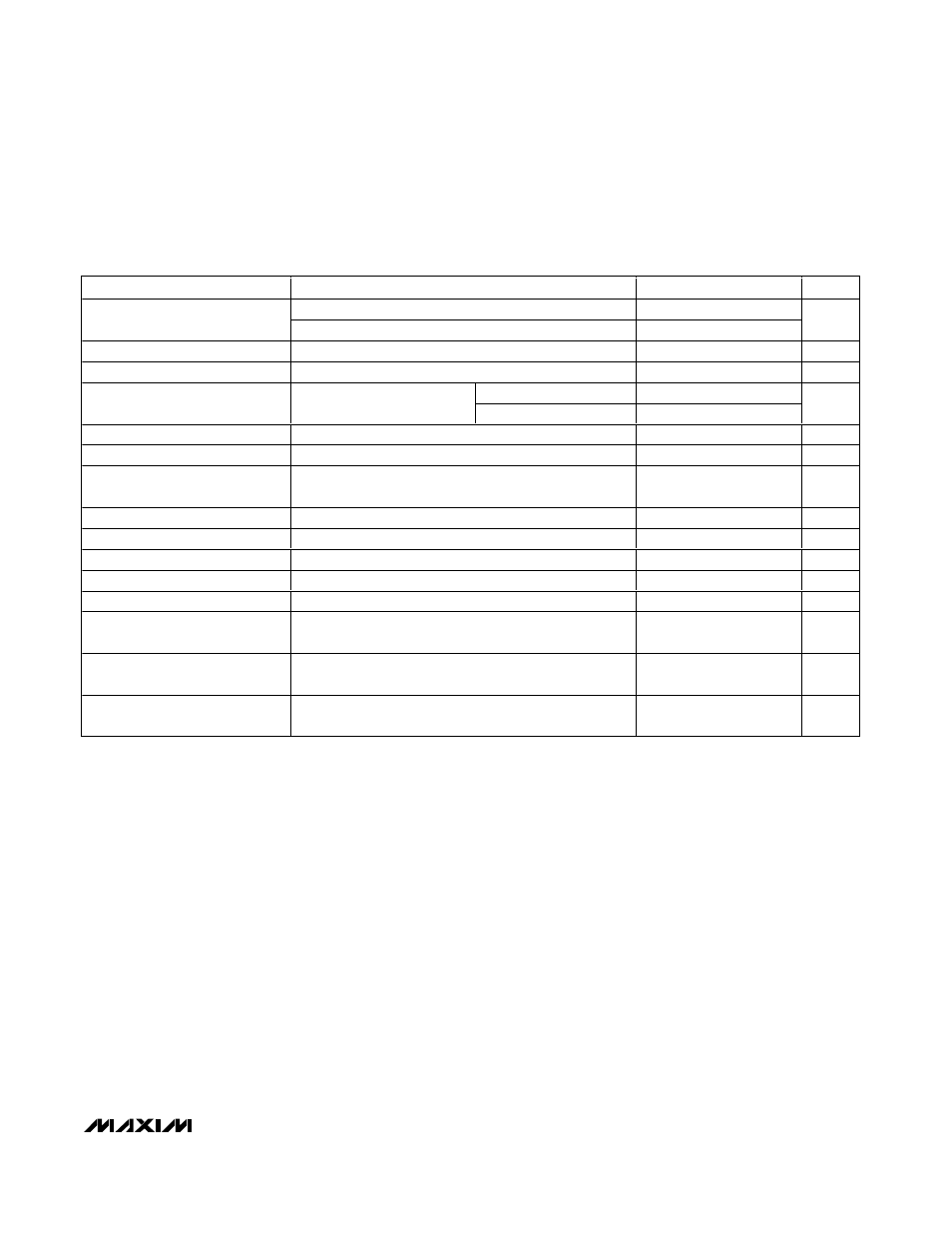
AC ELECTRICAL CHARACTERISTICS (continued)
(Typical Operating Circuit with one attenuator connected, V
CC
= +4.75V to +5.25V, T
A
= -40°C to +85°C, unless otherwise noted.
Typical values are at V
CC
= +5.0V, R1 = 1.2k
Ω, R2 = 2kΩ, P
OUT
= +5dBm, f
IN
= 2100MHz, V
CNTL
= 1V, 50
Ω system impedance,
second attenuator is not connected, T
A
= +25°C, unless otherwise noted.) (Note 3)
Note 1: Total supply current reduces as R
1
and R
2
are increased.
Note 2: Operating outside this range for extended periods may affect device reliability. Limit pin input current to 40mA when V
CC
is not present.
Note 3: All limits include external component losses, unless otherwise noted.
Note 4: Noise figure increases by approximately 1dB for every 1dB of gain reduction.
Note 5: f
1
= 2100MHz, f
2
= 2101MHz, +5dBm/tone at OUT.
Note 6: Switching time is measured from 50% of the control signal to when the RF output settles to ±1dB.
PARAMETER
CONDITIONS
MIN
TYP
MAX
UNITS
T
A
= +25°C to +85°C
-0.83
Output 3rd-Order Intercept Point
Variation Over Temperature
T
A
= +25°C to -40°C
-0.6
dB
2nd Harmonic
From maximum gain to 15dB attenuation, P
OUT
= +5dBm
-65
dBc
3rd Harmonic
From maximum gain to 15dB attenuation, P
OUT
= +5dBm
-83
dBc
One attenuator
17
20.7
RF Gain-Control Range
f
RF
= 1.7GHz to 2.2GHz,
V
CNTL
= 1V to 4.5V
Two attenuators
34
42.4
dB
RF Gain-Control Slope
V
CNTL
= 1.8V to 3.5V
-10
dB/V
Maximum RF Gain-Control Slope
Maximum slope vs. gain-control voltage
-15.2
dB/V
Gain Flatness Over
100MHz Bandwidth
Peak-to-peak for all settings
0.5
dB
Attenuator Switching Time
15dB attenuation change (Note 6)
500
ns
Attenuator Insertion Loss
Second attenuator (IN_A, OUT_A)
2.2
dB
Input Return Loss
Entire band, all gain settings
18
dB
Output Return Loss
Entire band, all gain settings
15
dB
Group Delay
Input/output 50
Ω lines de-embedded
300
ps
Group Delay Flatness Over
100MHz Bandwidth
Peak to peak
20
ps
Group Delay Change vs. Gain
Control
V
CNTL
= 1V to 4V
-70
ps
Insertion Phase Change vs. Gain
Control
V
CNTL
= 1V to 4V
50
degrees