Rainbow Electronics MAX1425 User Manual
Page 2
MAX1425
10-Bit, 20Msps ADC
2
_______________________________________________________________________________________
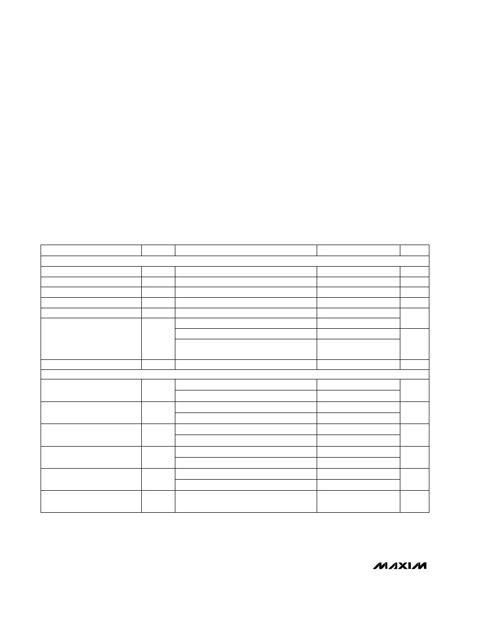
ABSOLUTE MAXIMUM RATINGS
ELECTRICAL CHARACTERISTICS
(V
AVDD
= V
CMLP
= +5V, V
DVDD
= +3.3V, V
CMLN
= V
AGND
= V
DGND
= 0, internal reference, digital output load = 35pF, f
CLK
= 20MHz
(50% duty cycle), T
A
= T
MIN
to T
MAX
, unless otherwise noted. Typical values are at T
A
= +25°C.)
Stresses beyond those listed under “Absolute Maximum Ratings” may cause permanent damage to the device. These are stress ratings only, and functional
operation of the device at these or any other conditions beyond those indicated in the operational sections of the specifications is not implied. Exposure to
absolute maximum rating conditions for extended periods may affect device reliability.
AV
DD
to AGND ........................................................ -0.3V to +6V
DV
DD
to DGND ....................................................... -0.3V to +6V
AV
DD
to DGND ........................................................ -0.3V to +6V
DGND to AGND ................................................................. ±0.3V
REFP, REFIN, REFN, CMLN, CMLP,
CML, INP, INN ....................(V
AGND
- 0.3V) to (V
AVDD
+ 0.3V)
CLK, OE/PD, D0–D9 ...............(V
DGND
- 0.3V) to (V
DVDD
+ 0.3V)
Continuous Power Dissipation (T
A
= +70°C)
28-Pin SSOP (derated 9.5mW/°C above +70°C) .........762mW
Operating Temperature Ranges
MAX1425CAI ..................................................... 0°C to +70°C
MAX1425EAI................................................... -40°C to +85°C
Junction Temperature ..................................................... +150°C
Storage Temperature Range ............................-65°C to +150°C
Lead Temperature (soldering, 10s) .................................+300°C
SINAD
dB
PARAMETER
SYMBOL
MIN
TYP
MAX
UNITS
Gain Error
GE
-10
±5
10
Midscale Offset
MSO
-3
±1.0
3
No Missing Codes
Integral Nonlinearity
INL
-1.5
±0.3
1.5
LSB
-5
±2
5
-5
±3 5
Power-Supply Rejection Ratio
PSRR
-5
±2
5
mV/V
Resolution
RES
10
Bits
Differential Nonlinearity
DNL
-1
1
LSB
Signal-to-Noise Ratio
SNR
60
61
dB
Spurious-Free Dynamic Range
SFDR
70
72
dB
Total Harmonic Distortion
(first five harmonics)
THD
-70
-67
dB
Signal-to-Noise and Distortion
59
61
CONDITIONS
f = 2MHz
Internal reference (Note 1)
(Note 1)
Guaranteed monotonic
External reference (REFIN) (Note 2)
External reference (REFP, CML, REFN)
(Note 3)
(Note 4)
f = 2MHz
f = 2MHz
f = 2MHz
%FSR
%FSR
f = 10MHz
56
59
f = 10MHz
64
69
f = 10MHz
-69
-64
f = 10MHz
55
59
ENOB
Bits
Effective Number of Bits
9.3
9.7
f = 2MHz
f = 10MHz
8.8
9.5
IMD
dBc
Intermodulation Distortion
-70
f1 = 10.17MHz, f2 = 10.19MHz
(-7dB FS, each tone) (Note 5)
ACCURACY
DYNAMIC PERFORMANCE (V
INP
- V
INN
= +2V to -2V)