Rainbow Electronics MAX1425 User Manual
Page 11
MAX1425
10-Bit, 20Msps ADC
______________________________________________________________________________________
11
and REFN. In this mode, the voltages at these pins
are set to their nominal values (see Electrical
Characteristics). The reference voltage levels can be
adjusted externally by applying a voltage at REFIN.
This allows other input levels to be used as well. The
full external reference mode is entered when REFIN =
AGND. External voltages can be applied to REFP,
CML, and REFN. In this mode, the internal reference
shuts down, resulting in less overall power consump-
tion.
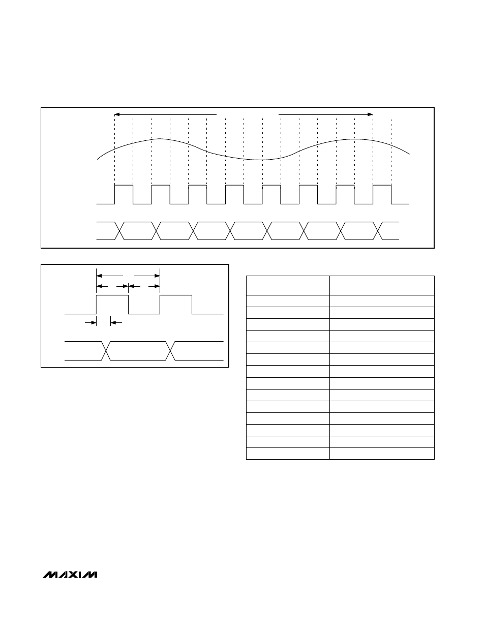
Clock Input (CLK)
CLK is TTL/CMOS-compatible. Since the interstage
conversion of the device depends on the rising and
falling edges of the external clock, use a clock with low
jitter and fast rise and fall times (<2ns). Low clock jitter
improves SNR performance. The MAX1425 operates
with a 50% duty cycle. If the clock has a duty cycle
other than 50%, the clock must meet the specifications
for high and low periods as stated in the Electrical
Characteristics.
Output Enable/Power-Down Function
(
OE
/PD) and Output Data
All data outputs, D0 through D9, are TTL/CMOS-logic
compatible. There is a 5.5 clock-cycle latency between
the start convert signal and the valid output data. The
output coding for the MAX1425 is in binary two’s com-
plement format, which has the MSB inverted (Table 1).
The digital output goes into a high-impedance state
and the device into a low-power mode when OE/PD
goes high. For normal operation, drive OE low. The out-
puts are not designed to drive high capacitances or
n - 6
n
n - 5
n + 1
n - 4
n + 2
n - 3
n + 3
n - 2
n + 4
n - 1
n + 5
n
n + 6
n + 1
n + 7
5.5 CLOCK-CYCLE LATENCY
ANALOG INPUT
CLOCK INPUT
DATA OUTPUT
Figure 3. System Timing Diagram
Figure 4. Output Timing Diagram
DATA 0
INPUT
CLK
OUTPUT
DATA
t
OD
t
CLK
t
CH
t
CI
DATA 1
DATA 2
1 1 1 1 1 1 1 1 1 1
-1 LSB
1 1 1 0 0 0 0 0 0 0
-1/4 Full Scale
1 1 0 0 0 0 0 0 0 0
-1/2 Full Scale
0 1 0 0 0 0 0 0 0 0
+1/2 Full Scale
0 0 1 0 0 0 0 0 0 0
+1/4 Full Scale
0 0 0 0 0 0 0 0 0 1
+1 LSB
0 0 0 0 0 0 0 0 0 0
Bipolar Zero
0 1 1 0 0 0 0 0 0 0
+3/4 Full Scale
0 1 1 1 1 1 1 1 0 1
+Full Scale 2LSB
0 1 1 1 1 1 1 1 1 0
+Full Scale 1LSB
0 1 1 1 1 1 1 1 1 1
+Full Scale
OUTPUT CODE
(TWO’S COMPLEMENT)
DIFFERENTIAL INPUT
Table 1. MAX1425 Output Code
1 0 1 0 0 0 0 0 0 0
-3/4 Full Scale
1 0 0 0 0 0 0 0 0 1
-Full Scale + 1LSB
1 0 0 0 0 0 0 0 0 0
-Full Scale