Detailed description – Rainbow Electronics MAX1425 User Manual
Page 10
MAX1425
10-Bit, 20Msps ADC
10
______________________________________________________________________________________
Detailed Description
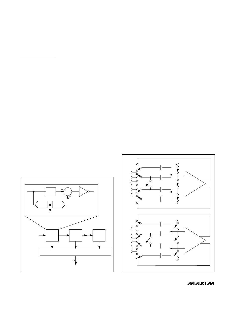
The MAX1425 uses a 10-stage, fully differential, pipelined
architecture (Figure 1) that allows for high-speed conver-
sion while minimizing power consumption. Each sample
moves through a pipeline stage every half clock cycle.
Counting the delay through the output latch, there is a 5.5
clock-cycle latency.
A 2-bit flash ADC converts the input voltage to digital
code. A DAC converts the ADC result back into an ana-
log voltage, which is subtracted from the held input sig-
nal. The resulting error signal is then multiplied by two,
and this product is passed along to the next pipeline
stage where the process is repeated. Digital error correc-
tion compensates for offsets and mismatches in each
pipeline stage and ensures no missing codes.
Internal Track-and-Hold Circuit
Figure 2 shows a simplified functional diagram of the
internal track-and-hold (T/H) circuit in both track mode
and hold mode. The fully differential circuit samples the
input signal onto the four capacitors C1a, C1b, C2a,
and C2b. Switches S2a and S2b set the common mode
for the amplifier input, and open before S1. When S1
opens, the input is sampled. Switches S3a and S3b
then connect capacitors C1a and C1b to the output of
the amplifier. Capacitors C2a and C2b are connected
either to REFN, REFP, or each other, depending on the
results of the flash ADC. The amplifier then multiplies
the residue by two and the next stage in the pipeline
performs a similar operation.
System Timing Requirements
Figure 3 shows the relationship between the clock
input, analog input, and data output. The MAX1425
samples the falling edge of the input clock. Output data
is valid on the rising edge of the input clock. The output
data has an internal latency of 5.5 clock cycles, as
shown. Figure 4 shows an output timing diagram that
specifies the relationship between the input clock para-
meters and the valid output data.
Analog Input and Internal Reference
The MAX1425 has an internal +2.5V reference used to
generate three reference levels: +3.25V, +2.25V, and
+1.25V corresponding to V
REFP
, V
CML
, and V
REFN
.
These reference voltages enable a ±2V input range.
Bypass all reference voltages with a 0.1µF capacitor.
The MAX1425 allows for three modes of reference
operation: an internal reference (default) mode, an
externally adjusted reference mode, or a full external
reference mode. The internal reference mode occurs
when no voltages are applied to REFIN, REFP, CML,
T/H
V
OUT
x2
Σ
FLASH
ADC
DAC
2 BITS
MDAC
10
V
IN
V
IN
STAGE 1
STAGE 2
D [9:0]
DIGITAL CORRECTION LOGIC
STAGE 10
S3a
INP
REFP
REFN
REFP
REFN
INN
S4a
S4c
C1a
CML
S2a
S1
S2b
CML
C2a
C2b
C1b
S4b
S3a
INP
a) TRACK MODE
b) HOLD MODE
REFP
REFN
REFP
REFN
INN
S4a
S3b
S4c
C1a
CML
S2a
S1
S2b
CML
C2a
C2b
C1b
S4b
Figure 1. Pipelined A/D Architecture (Block)
Figure 2. Internal Track-and-Hold Circuit