Applications information – Rainbow Electronics MAX1425 User Manual
Page 12
MAX1425
10-Bit, 20Msps ADC
12
______________________________________________________________________________________
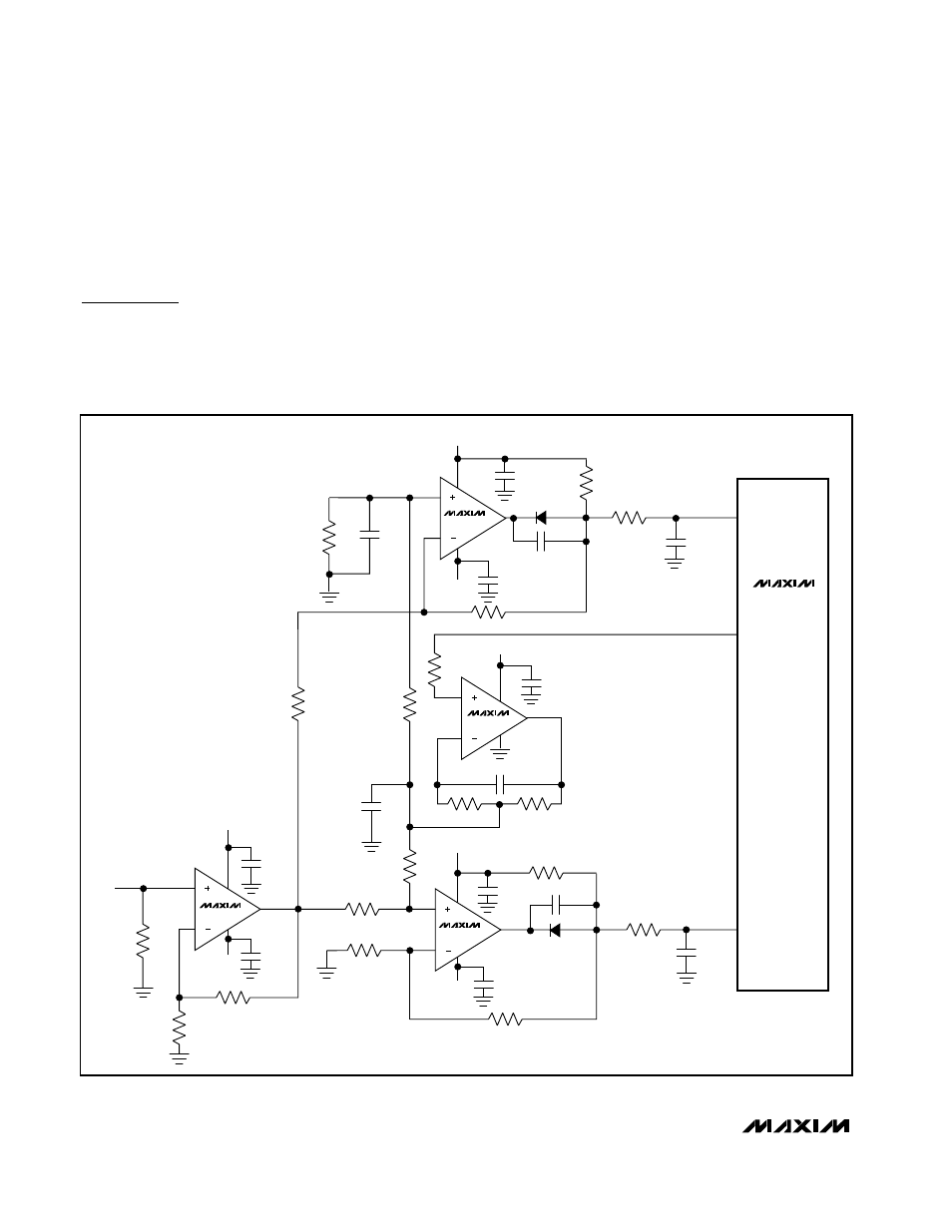
Figure 5. Typical Application Circuit Using the Internal Reference
INPUT
50
Ω
25
Ω
-5V
+5V
0.1
µF
0.1
µF
0.1
µF
BAS16
22pF
+5V
-5V
300
Ω
600
Ω
300
Ω
300
Ω
INP
CML
INN
600
Ω
2.5k
+5V
-5V
0.1
µF
600
Ω
300
Ω
300
Ω
600
Ω
300
Ω
50
Ω
50
Ω
2.5k
+5V
22pF
50
Ω
BAS16
0.1
µF
0.1
µF
0.1
µF
0.1
µF
0.1
µF
0.1
µF
0.1
µF
0.1
µF
25
Ω
MAX4108
MAX473A
MAX1425
MAX4108
MAX4108
heavy loads, as they are specified to deliver only
200µA for TTL compatibility. If an application needs
output buffering, use 74LS74s or 74ALS541s as
required.
Applications Information
Figure 5 depicts a typical application circuit containing
a single-ended to differential converter. The internal ref-
erence provides a +2.25V output for level shifting. The
input is buffered and then split to a voltage follower and
inverter. The op amps are followed by a lowpass filter
to remove some of the wideband noise associated with
high-speed op amps. In this application, the amplifier
outputs are directly coupled to the inputs. This configura-
tion can also be modified for AC-coupled applications.
The MAX1425 includes a DC level-shifting circuit internal
to the part, allowing for AC-coupled applications. The
level-shifting circuit is shown in Figure 6.
The circuit in Figure 6 can accept a 1Vp-p maximum
input voltage. With a maximum clock frequency of
20MHz, use 50
Ω termination to minimize reflections.
Buffer the digital outputs with a low-cost, high-speed,