Logic electrical characteristics, Smbus digital switching characteristics, Lm99 – Rainbow Electronics LM99 User Manual
Page 5
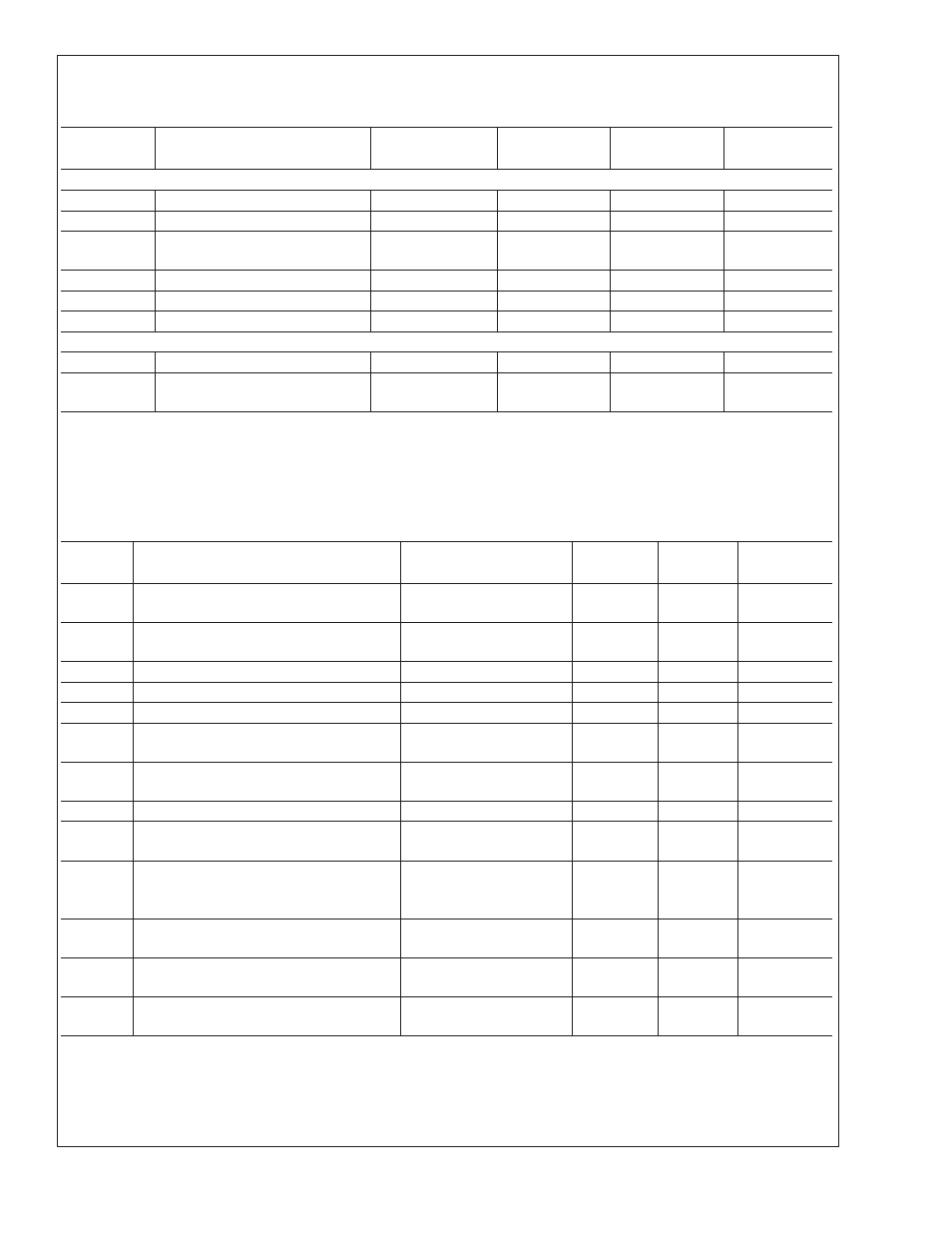
Logic Electrical Characteristics
DIGITAL DC CHARACTERISTICS Unless otherwise noted, these specifications apply for V
DD
= +3.0 to 3.6 Vdc. Boldface
limits apply for T
A
= T
J
= T
MIN
to T
MAX
; all other limits T
A
= T
J
= +25˚C, unless otherwise noted.
Symbol
Parameter
Conditions
Typical
Limits
Units
(Limit)
SMBData, SMBCLK INPUTS
V
IN(1)
Logical “1” Input Voltage
2.1
V (min)
V
IN(0)
Logical “0”Input Voltage
0.8
V (max)
V
IN(HYST)
SMBData and SMBCLK Digital
Input Hysteresis
400
mV
I
IN(1)
Logical “1” Input Current
V
IN
= V
DD
0.005
±
10
µA (max)
I
IN(0)
Logical “0” Input Current
V
IN
= 0 V
−0.005
±
10
µA (max)
C
IN
Input Capacitance
5
pF
ALL DIGITAL OUTPUTS
I
OH
High Level Output Current
V
OH
= V
DD
10
µA (max)
V
OL
SMBus Low Level Output Voltage
I
OL
= 4 mA
I
OL
= 6 mA
0.4
0.6
V (max)
SMBus Digital Switching Characteristics
Unless otherwise noted, these specifications apply for V
DD
= +3.0 Vdc to +3.6 Vdc, C
L
(load capacitance) on output lines = 80
pF. Boldface limits apply for T
A
= T
J
= T
MIN
to T
MAX
; all other limits T
A
= T
J
= +25˚C, unless otherwise noted. The switch-
ing characteristics of the LM99 fully meet or exceed the published specifications of the SMBus version 2.0. The following pa-
rameters are the timing relationships between SMBCLK and SMBData signals related to the LM99. They adhere to but are not
necessarily the SMBus bus specifications.
Symbol
Parameter
Conditions
Typical
Limits
Units
(Limit)
f
SMB
SMBus Clock Frequency
100
10
kHz (max)
kHz (min)
t
LOW
SMBus Clock Low Time
from V
IN(0)
max to
V
IN(0)
max
4.7
25
µs (min)
ms (max)
t
HIGH
SMBus Clock High Time
from V
IN(1)
min to V
IN(1)
min
4.0
µs (min)
t
R,SMB
SMBus Rise Time
1
µs (max)
t
F,SMB
SMBus Fall Time
0.3
µs (max)
t
OF
Output Fall Time
C
L
= 400 pF,
I
O
= 3 mA, (Note 13)
250
ns (max)
t
TIMEOUT
SMBData and SMBCLK Time Low for
Reset of Serial Interface (Note 14)
25
35
ms (min)
ms (max)
t
SU;DAT
Data In Setup Time to SMBCLK High
250
ns (min)
t
HD;DAT
Data Out Stable after SMBCLK Low
300
900
ns (min)
ns (max)
t
HD;STA
Start Condition SMBData Low to SMBCLK
Low (Start condition hold before the first
clock falling edge)
100
ns (min)
t
SU;STO
Stop Condition SMBCLK High to SMBData
Low (Stop Condition Setup)
100
ns (min)
t
SU;STA
SMBus Repeated Start-Condition Setup
Time, SMBCLK High to SMBData Low
0.6
µs (min)
t
BUF
SMBus Free Time Between Stop and Start
Conditions
1.3
µs (min)
LM99
www.national.com
5