Ac electrical characteristics—max2683 – Rainbow Electronics MAX2684 User Manual
Page 2
MAX2683/MAX2684
3.5GHz Downconverter Mixers
with Selectable LO Doubler
2
_______________________________________________________________________________________
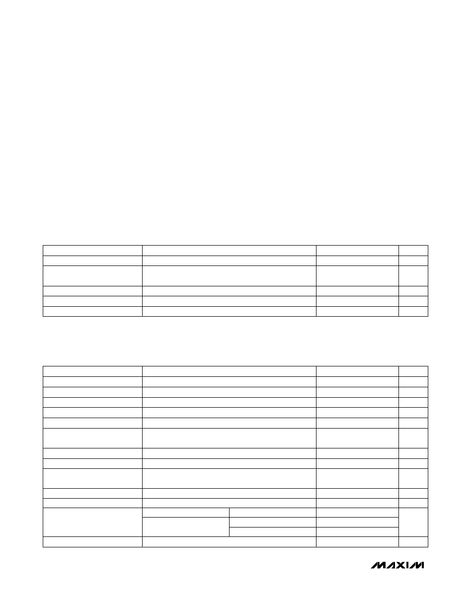
ABSOLUTE MAXIMUM RATINGS
DC ELECTRICAL CHARACTERISTICS
(V
CC
= +2.7V to +5.5V; R
BIAS
= 1.2k
Ω; ENX2 = GND; RFIN, LOX1, and LOX2 are terminated in 50Ω, no input signal applied; IFOUT+
= IFOUT- = V
CC
, T
A
= -40°C to +85°C, unless otherwise noted. Typical values are at V
CC
= +5V, T
A
= +25°C.) (Note 1)
AC ELECTRICAL CHARACTERISTICS—MAX2683
(MAX2683/MAX2684 EV kit, V
CC
= +5V, R
BIAS
= 1.2k
Ω, ENX2 = GND, f
RF
= 3.6GHz, P
RF
= -20dBm, f
LOX2
= 1650MHz, P
LO
= -5dBm,
all input/output ports terminated in 50
Ω, IFOUT+ and IFOUT- matched to single-ended 50Ω load, T
A
= +25°C, unless otherwise noted.)
Stresses beyond those listed under “Absolute Maximum Ratings” may cause permanent damage to the device. These are stress ratings only, and functional
operation of the device at these or any other conditions beyond those indicated in the operational sections of the specifications is not implied. Exposure to
absolute maximum rating conditions for extended periods may affect device reliability.
V
CC
to GND ...........................................................-0.3V to +6.0V
IFOUT+, IFOUT-, ENX2, BIAS to GND .......-0.3V to (V
CC
+ 0.3V)
RFIN Input Power (50
Ω source) .....................................+10dBm
LO Input Power (50
Ω source) ........................................+10dBm
R
BIAS
.............................................................................820
Ω min
Continuous Power Dissipation (T
A
= +70°C)
16-pin TSSOP-EP (derate 21.3mW/°C
above +70°C).............................................................1702mW
Operating Temperature Range ...........................-40°C to +85°C
Junction Temperature ......................................................+150°C
Storage Temperature Range ..............................-65°C to+150°C
Lead Temperature (soldering, 10s) .................................+300°C
PARAMETER
MIN
TYP
MAX
UNITS
Gain Variation Over
Temperature
±0.5
±1.2
dB
Conversion Gain
4.8
6.7
8.0
dB
Input 1dB Compression Point
+0.8
dBm
Input Third-Order Intercept Point
+8.8
dBm
Input Second-Order Intercept
Point
+33
dBm
Noise Figure
12
dB
IF Frequency Range
RF Frequency Range
3.4
3.8
GHz
100
400
MHz
LOX1 Frequency Range
3.0
3.9
GHz
RFIN Input Return Loss
-18
dB
LOX2 Leakage at RFIN
-42
dBm
-38
-49
LOX1 Leakage at RFIN
-39
dBm
CONDITIONS
(Note 8)
T
A
= -40°C to +85°C (Note 2)
f
RFIN
= 3
×
f
LO
(Notes 1, 4)
(Note 5)
(Note 6)
(Note 7)
(Notes 2, 3)
(Notes 2, 3)
ENX2 = V
CC
(Notes 2, 3)
f
RFIN
= 2
×
f
LO
f
RFIN
= 1
×
f
LO
ENX2 = GND
LOX2 Frequency Range
1.5
1.95
GHz
ENX2 = GND (Notes 2, 3)
ENX2 = V
CC
, f
RFIN
= 1
×
f
LO,
f
LOX1
= 3.3GHz
PARAMETER
MIN
TYP
MAX
UNITS
Input Logic Bias Current
-20
10
µA
Input Logic Voltage Low
0.6
V
Supply Current Reduction when
LO Doubler is Disabled
Supply Current
55
66
mA
15
mA
Input Logic Voltage High
2.0
V
CONDITIONS
ENX2 = V
CC