Electrical characteristics (continued) – Rainbow Electronics MAX1418 User Manual
Page 3
MAX1418
15-Bit, 65Msps ADC with -78.2dBFS
Noise Floor for IF Applications
_______________________________________________________________________________________
3
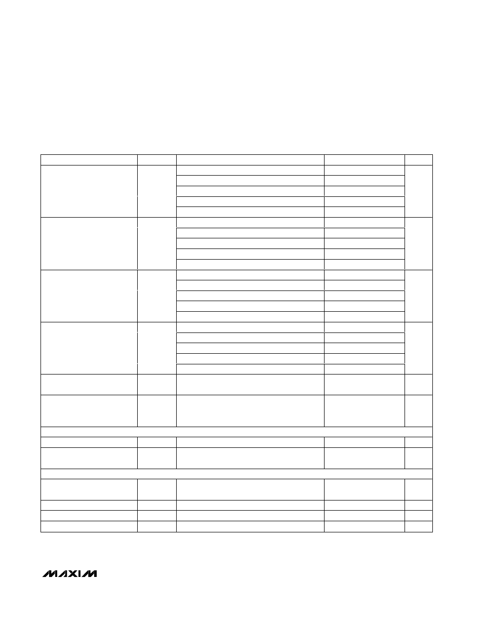
ELECTRICAL CHARACTERISTICS (continued)
(AV
CC
= 5V, DV
CC
= DRV
CC
= 2.5V, GND = 0, INP and INN driven differentially with -2dBFS, CLKP and CLKN driven differentially
with a 2V
P-P
sinusoidal input signal, C
L
= 5pF at digital outputs, f
CLK
= 65MHz, T
A
= T
MIN
to T
MAX
, unless otherwise noted. Typical
values are at T
A
= +25°C, unless otherwise noted. ≥+25°C guaranteed by production test, <+25°C guaranteed by design and char-
acterization.)
PARAMETER
SYMBOL
CONDITIONS
MIN
TYP
MAX
UNITS
f
IN
= 5MHz at -2dBFS
75
f
IN
= 15MHz at -2dBFS
75
f
IN
= 35MHz at -2dBFS
74.8
f
IN
= 70MHz at -2dBFS
72
73.6
Signal-to-Noise Ratio (Note 1)
SNR
f
IN
= 170MHz at -6dBFS
68.5
dB
f
IN
= 5MHz at -2dBFS
74.8
f
IN
= 15MHz at -2dBFS
74.8
f
IN
= 35MHz at -2dBFS
74.4
f
IN
= 70MHz at -2dBFS
71
73.3
Signal-to-Noise and Distortion
(Note 2)
SINAD
f
IN
= 170MHz at -6dBFS
64.4
dB
f
IN
= 5MHz at -2dBFS
90
f
IN
= 15MHz at -2dBFS
90
f
IN
= 35MHz at -2dBFS
88
f
IN
= 70MHz at -2dBFS
78
88
Spurious-Free Dynamic Range
(HD2 and HD3)
(Note 2)
SFDR1
f
IN
= 170MHz at -6dBFS
67.5
dBc
f
IN
= 5MHz at -2dBFS
95
f
IN
= 15MHz at -2dBFS
95
f
IN
= 35MHz at -2dBFS
93
f
IN
= 70MHz at -2dBFS
84.5
92
Spurious-Free Dynamic Range
(HD4 and Higher)
(Note 2)
SFDR2
f
IN
= 170MHz at -6dBFS
82
dBc
Two-Tone Intermodulation
Distortion
TTIMD
f
IN1
= 69MHz at -8dBFS;
f
IN2
= 71MHz at -8dBFS
-85
dBc
Two-Tone Spurious-Free
Dynamic Range
SFDR
TT
f
IN1
= 69MHz at -12dBFS < f
IN1
< -100dBFS;
f
IN2
= 71MHz at -12dBFS < f
IN2
< -100dBFS
(Note 2)
-100
dBFS
DIGITAL OUTPUTS (D0–D14, DAV, DOR)
Digital Output-Voltage Low
V
OL
0.5
V
Digital Output-Voltage High
V
OH
DV
CC
-
0.5
V
TIMING CHARACTERISTICS (DV
CC
= DRV
CC
= 2.5V)
Figure 4
CLKP/CLKN Duty Cycle
Duty cycle
50
±5
%
Effective Aperture Delay
t
AD
230
ps
Output Data Delay
t
DAT
(Note 3)
3.0
4.5
7.5
ns
Data Valid Delay
t
DAV
(Note 3)
5.3
6.5
8.7
ns