Rainbow Electronics MAX1418 User Manual
Page 12
MAX1418
15-Bit, 65Msps ADC with -78.2dBFS
Noise Floor for IF Applications
12
______________________________________________________________________________________
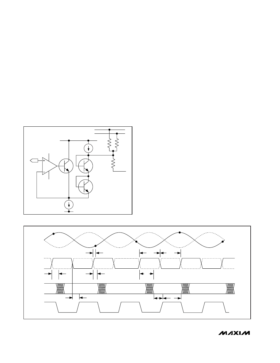
On-Chip Reference Circuit
The MAX1418 incorporates an on-chip 2.5V, low-drift
bandgap reference. This reference potential establish-
es the full-scale range for the converter, which is nomi-
nally 2.56V
P-P
differential. The internal reference
potential is not accessible to the user, so the full-scale
range for the MAX1418 cannot be externally adjusted.
Figure 3 shows how the reference is used to generate
the common-mode bias potential for the analog inputs.
The common-mode input bias is set to two diode poten-
tials above the bandgap reference potential, and so
varies over temperature.
Clock Inputs (CLKP, CLKN)
The differential clock buffer for the MAX1418 has been
designed to accept an AC-coupled clock waveform. Like
the signal inputs, the clock inputs are self-biasing. In this
case, the common-mode bias potential is 2.4V and each
input is connected to the reference potential through a
1kΩ resistor. Consequently, the differential input resis-
tance associated with the clock inputs is 2kΩ. While dif-
ferential clock signals as low as 0.5V
P-P
may be used to
drive the clock inputs, best dynamic performance is
achieved with clock input voltage levels of 2V
P-P
to 3V
P-P
.
Jitter on the clock signal translates directly to jitter (noise)
on the sampled signal. Therefore, the clock source
should be a low-jitter (low phase noise) source. See the
Applications Information section for additional details on
driving the clock inputs.
System Timing Requirements
Figure 4 depicts the timing relationships for the signal
input, clock input, data output, and DAV output. The
variables shown in the figure correspond to the various
timing specifications in the Electrical Characteristics
section. These include:
• t
DAT
: Delay from the rising edge of the clock until the
50% point of the output data transition
• t
DAV
: Delay from the falling edge of the clock until the
50% point of the DAV rising edge
• t
DNV
: Time from the rising edge of the clock until data
is no longer valid
• t
DGV
: Time from the rising edge of the clock until data
is guaranteed to be valid
1mA
2mA
INP/INN
COMMON-MODE
REFERENCE
500Ω
500Ω
1kΩ
2.5V
Figure 3. Simplified Reference Architecture
INP
INN
D0–D14
DOR
DAV
N + 1
N
N + 2
N + 3
CLKP
CLKN
t
AD
t
CLKP
t
CLKN
N - 3
N - 2
N - 1
N
t
S
t
H
t
DAT
t
DAV
t
DNV
t
DGV
Figure 4. System and Output Timing Diagram