Rainbow Electronics MAX1418 User Manual
Page 2
MAX1418
15-Bit, 65Msps ADC with -78.2dBFS
Noise Floor for IF Applications
2
_______________________________________________________________________________________
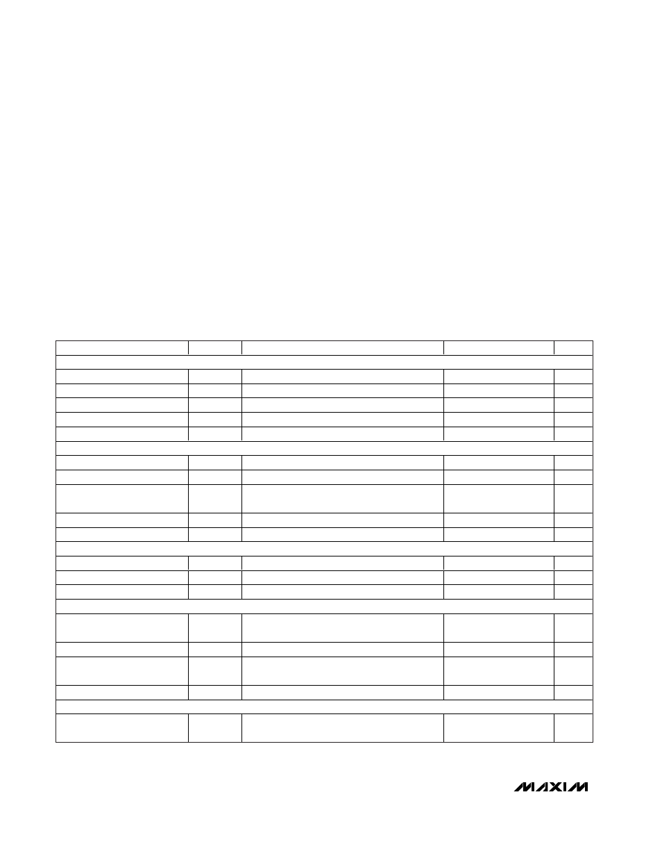
ABSOLUTE MAXIMUM RATINGS
ELECTRICAL CHARACTERISTICS
(AV
CC
= 5V, DV
CC
= DRV
CC
= 2.5V, GND = 0, INP and INN driven differentially with -2dBFS, CLKP and CLKN driven differentially
with a 2V
P-P
sinusoidal input signal, C
L
= 5pF at digital outputs, f
CLK
= 65MHz, T
A
= T
MIN
to T
MAX
, unless otherwise noted. Typical
values are at T
A
= +25°C, unless otherwise noted. ≥+25°C guaranteed by production test, <+25°C guaranteed by design and char-
acterization.)
Stresses beyond those listed under “Absolute Maximum Ratings” may cause permanent damage to the device. These are stress ratings only, and functional
operation of the device at these or any other conditions beyond those indicated in the operational sections of the specifications is not implied. Exposure to
absolute maximum rating conditions for extended periods may affect device reliability.
AV
CC
, DV
CC
, DRV
CC
to GND.................................. -0.3V to +6V
INP, INN, CLKP, CLKN, CM to GND........-0.3V to (AV
CC
+ 0.3V)
D0–D14, DAV, DOR to GND..................-0.3V to (DRV
CC
+ 0.3V)
Continuous Power Dissipation (T
A
= +70°C)
56-Pin Thin QFN (derate 47.6mW/°C above +70°C)................
3809.5mW
Operating Temperature Range ...........................-40°C to +85°C
Thermal Resistance
θJ
A
...................................................21°C/W
Junction Temperature ......................................................+150°C
Storage Temperature Range .............................-60°C to +150°C
PARAMETER
SYMBOL
CONDITIONS
MIN
TYP
MAX
UNITS
DC ACCURACY
Resolution
15
Bits
Integral Nonlinearity
INL
f
IN
= 15MHz
±1.5
LSB
Differential Nonlinearity
DNL
f
IN
= 70MHz, no missing codes guaranteed
±0.4
LSB
Offset Error
-12
+12
mV
Gain Error
-4
+4
%FS
ANALOG INPUT (INP, INN)
D i ffer enti al Inp ut V ol tag e Rang e
V
DIFF
Fully differential inputs drive, V
DIFF
= V
INP
- V
INN
2.56
V
P-P
Common-Mode Input Voltage
V
CM
Self-biased
4.17
V
Differential Input Resistance
R
IN
1
±15%
k
Ω
Differential Input Capacitance
C
IN
1
pF
Full-Power Analog Bandwidth
FPBW
-1dB
-1dB rolloff for a full-scale input
260
MHz
CONVERSION RATE
Maximum Clock Frequency
f
CLK
65
MHz
Minimum Clock Frequency
f
CLK
20
MHz
Aperture Jitter
t
AJ
0.21
ps
RMS
CLOCK INPUT (CLKP, CLKN)
Full-Scale Differential Input
Voltage
V
DIFFCLK
Fully differential input drive, V
CLKP
- V
CLKN
0.5 to
3.0
V
Common-Mode Input Voltage
V
CM
Self-biased
2.4
V
Differential Input Resistance
R
INCLK
2
±15%
k
Ω
Differential Input Capacitance
C
INCLK
1
pF
DYNAMIC CHARACTERISTICS
Thermal + Quantization
Noise Floor
NF
Analog input <-35dBFS
-78.2
dBFS