Rainbow Electronics MAX495 User Manual
Page 2
MAX492/MAX494/MAX495
Single/Dual/Quad, Micropower,
Single-Supply Rail-to-Rail Op Amps
2
_______________________________________________________________________________________
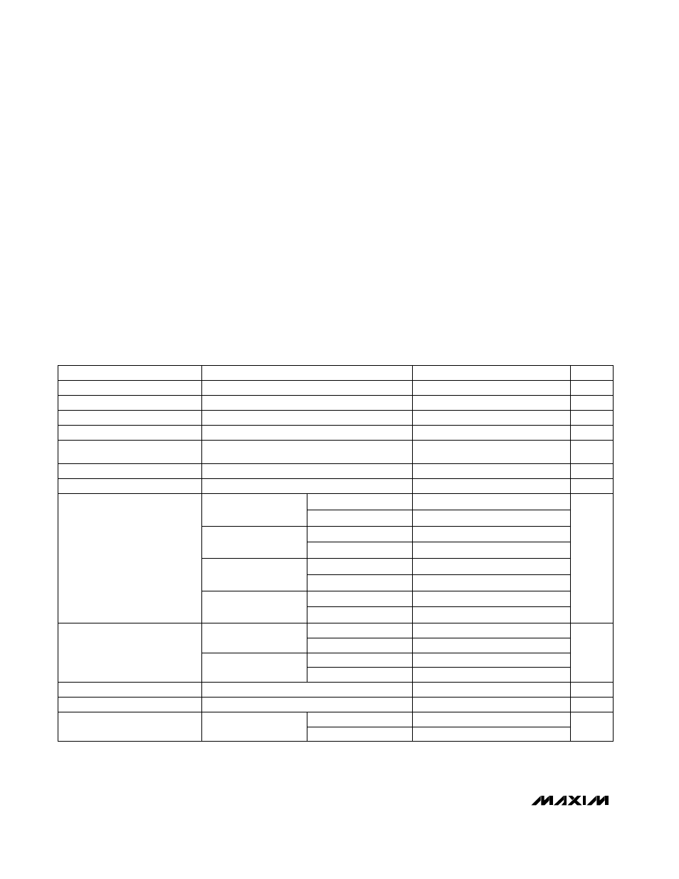
ABSOLUTE MAXIMUM RATINGS
DC ELECTRICAL CHARACTERISTICS
(V
CC
= 2.7V to 6V, V
EE
= GND, V
CM
= 0V, V
OUT
= V
CC
/ 2, T
A
= +25°C, unless otherwise noted.)
Stresses beyond those listed under “Absolute Maximum Ratings” may cause permanent damage to the device. These are stress ratings only, and functional
operation of the device at these or any other conditions beyond those indicated in the operational sections of the specifications is not implied. Exposure to
absolute maximum rating conditions for extended periods may affect device reliability.
Supply Voltage (V
CC
to V
EE
) ....................................................7V
Common-Mode Input Voltage..........(V
CC
+ 0.3V) to (V
EE
- 0.3V)
Differential Input Voltage .........................................±(V
CC
- V
EE
)
Input Current (IN+, IN-, NULL1, NULL2) ..........................±10mA
Output Short-Circuit Duration ....................Indefinite short circuit
to either supply
Voltage Applied to NULL Pins ....................................V
CC
to V
EE
Continuous Power Dissipation (T
A
= +70°C)
8-Pin Plastic DIP (derate 9.09mW/°C above +70°C) ....727mW
8-Pin SO (derate 5.88mW/°C above +70°C).................471mW
8-Pin CERDIP (derate 8.00mW/°C above +70°C).........640mW
8-Pin µMAX (derate 4.1mW/°C above +70°C) ..............330mW
14-Pin Plastic DIP (derate 10.00mW/°C above +70°C)...800mW
14-Pin SO (derate 8.33mW/°C above +70°C)...............667mW
14-Pin CERDIP (derate 9.09mW/°C above +70°C).......727mW
Operating Temperature Ranges
MAX49_C_ _ ........................................................0°C to +70°C
MAX49_E_ _......................................................-40°C to +85°C
MAX49_M_ _ ...................................................-55°C to +125°C
Junction Temperatures
MAX49_C_ _/E_ _..........................................................+150°C
MAX49_M_ _ .................................................................+175°C
Storage Temperature Range .............................-65°C to +150°C
Lead Temperature (soldering, 10sec) .............................+300°C
V
CM
= V
EE
to V
CC
V
CM
= V
OUT
= V
CC
/ 2
V
CM
= V
EE
to V
CC
V
CM
= V
EE
to V
CC
V
CC
= 2.7V,
R
L
= 100k
Ω
,
V
OUT
= 0.25V to 2.45V
V
CC
= 2.7V to 6V
(V
EE
- 0.25V)
≤
V
CM
≤
(V
CC
+ 0.25V)
R
L
= 100k
Ω
CONDITIONS
µA
135
150
Supply Current (per amplifier)
V
2.7
6.0
Operating Supply Voltage Range
mA
30
Output Short-Circuit Current
V
EE
+ 0.04 V
EE
+ 0.075
V
V
CC
- 0.075 V
CC
- 0.04
Output Voltage Swing
(Note 1)
nA
±0.5
±6
Input Offset Current
nA
±25
±60
µV
±200
±500
Input Offset Voltage
Input Bias Current
90
102
dB
90
104
Large-Signal Voltage Gain
(Note 1)
dB
88
110
Power-Supply Rejection Ratio
M
Ω
2
Differential Input Resistance
V
V
EE
- 0.25
V
CC
+ 0.25
Common-Mode Input
Voltage Range
74
90
UNITS
MIN
TYP
MAX
PARAMETER
Sourcing
Sinking
V
CC
= 2.7V, R
L
= 1k
Ω
,
V
OUT
= 0.5V to 2.2V
Sourcing
Sinking
78
90
94
105
V
CC
= 5.0V,
R
L
= 100k
Ω
,
V
OUT
= 0.25V to 4.75V
Sourcing
Sinking
92
100
98
108
V
CC
= 5.0V, R
L
= 1k
Ω
,
V
OUT
= 0.5V to 4.5V
Sourcing
Sinking
86
98
98
110
V
OH
V
OL
V
OH
V
OL
R
L
= 1k
Ω
V
EE
+ 0.15 V
EE
+ 0.20
V
CC
- 0.20
V
CC
- 0.15
150
170
V
CC
= 2.7V
V
CC
= 5V
Common-Mode Rejection Ratio
dB