Input stage protection circuitry – Rainbow Electronics MAX495 User Manual
Page 11
MAX492/MAX494/MAX495
Single/Dual/Quad, Micropower,
Single-Supply Rail-to-Rail Op Amps
the op amp in an inverting configuration (Figure 3a);
connect resistor R3 between the noninverting input and
the input signal when using the op amp in a noninvert-
ing configuration (Figure 3b). Select R3 to equal the
parallel combination of R1 and R2. High source resis-
tances will degrade noise performance, due to the ther-
mal noise of the resistor and the input current noise
(which is multiplied by the source resistance).
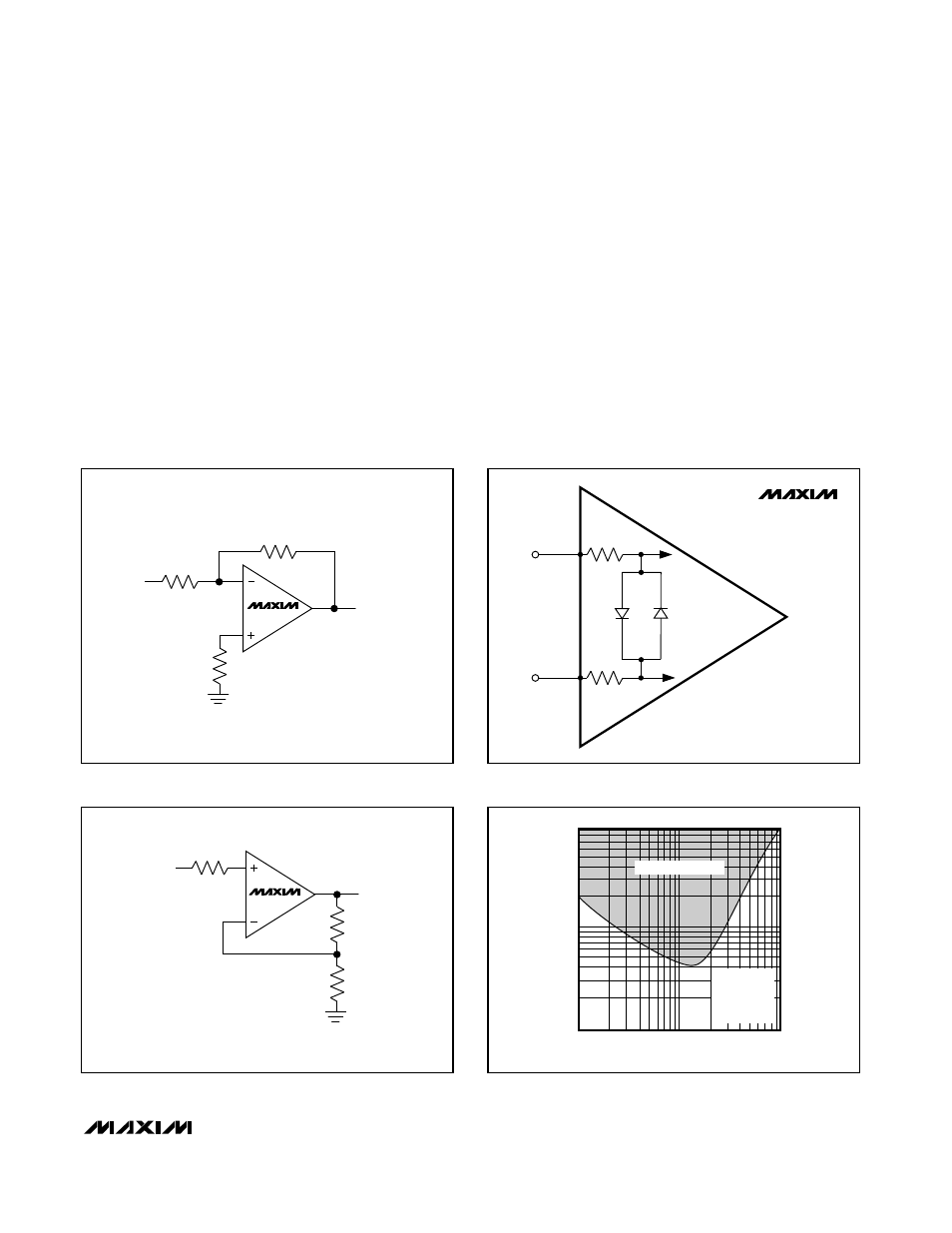
Input Stage Protection Circuitry
T
he MAX492/MAX494/MAX495 include internal protec-
tion circuitry that prevents damage to the precision
input stage from large differential input voltages. This
protection circuitry consists of back-to-back diodes
between IN+ and IN- with two 1.7k
Ω
resistors in series
(Figure 4). The diodes limit the differential voltage
applied to the amplifiers’ internal circuitry to no more
than V
F
, where V
F
is the diodes’ forward-voltage drop
(about 0.7V at +25°C).
Input bias current for the ICs (±25nA typical) is speci-
fied for the small differential input voltages. For large
differential input voltages (exceeding V
F
), this protec-
tion circuitry increases the input current at IN+ and IN-:
(V
IN
+ - V
IN
- ) - V
F
Input Current = ———————————
2 x 1.7k
Ω
For comparator applications requiring large differential
voltages (greater than V
F
), you can limit the input cur-
rent that flows through the diodes with external resistors
R1
V
OUT
R3 = R2
II
R1
R3
V
IN
R2
MAX49_
Figure 3a. Reducing Offset Error Due to Bias Current:
Inverting Configuration
R3
V
OUT
R3 = R2
II
R1
V
IN
R1
R2
MAX49_
MAX492
MAX494
MAX495
1.7k
Ω
1.7k
Ω
TO INTERNAL
CIRCUITRY
TO INTERNAL
CIRCUITRY
IN–
IN+
Figure 4. Input Stage Protection Circuitry
10,000
100
1
10
100
MAX492-FG 04
RESISTIVE LOAD (k
Ω
)
CAPACITIVE LOAD (pF)
1000
UNSTABLE REGION
V
CC
= +5V
V
OUT
= V
CC
/2
R
L
TO V
EE
A
V
= +1
Figure 5. Capacitive-Load Stable Region Sourcing Current
______________________________________________________________________________________
11
Figure 3b. Reducing Offset Error Due to Bias Current:
Noninverting Configuration