Max1747 triple charge-pump tft lcd dc-dc converter, Main charge pump, Dual charge-pump regulators – Rainbow Electronics MAX1747 User Manual
Page 9

MAX1747
Triple Charge-Pump TFT LCD
DC-DC Converter
_______________________________________________________________________________________
9
(V
POS
) and a negative output (V
NEG
). These two out-
puts use external diode and capacitor stages (as many
stages as required) to regulate output voltages above
+35V and under -35V.
A proprietary regulation algorithm minimizes output rip-
ple as well as capacitor sizes for all three charge
pumps. Also included in the MAX1747 are a precision
1.25V reference that sources up to 50µA, shutdown,
power-up sequencing, fault detection, and an active-
low open-drain ready output.
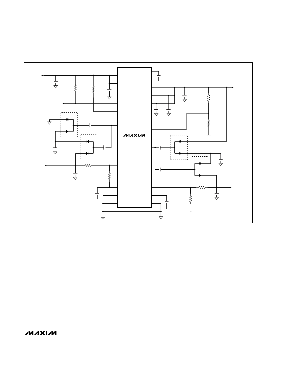
Main Charge Pump
During the first half-cycle, the MAX1747 charges the
flying capacitor (CX) by connecting it between the sup-
ply voltage (V
SUPM
) and ground (Figure 2). This initial
charge is controlled by the variable N-channel on-resis-
tance. During the second half-cycle, the MAX1747 level
shifts the flying capacitor by stacking the voltage
across CX on top of the supply voltage. This transfers
the sum of the two voltages to the output capacitor
(C
OUT
).
Dual Charge-Pump Regulators
The MAX1747 contains two individual low-power
charge pumps. Using a single stage, the first charge
pump inverts the supply voltage (V
SUPN
) and provides
a regulated negative output voltage. The second
charge pump doubles the supply voltage (V
SUPP
) and
provides a regulated positive output voltage. The
MAX1747 contains internal P-channel and N-channel
MOSFETs to control the power transfer. The internal
MOSFETs switch at a constant frequency set by the
current into the shutdown pin (see Frequency Selection
and Shutdown).
V
OUT
+5V, 200mA
V
IN
= 3.0V
D6
D5
D8
CIN
10
µF
R7
100k
R
FREQ
100k
C1
0.1
µF
C5
0.1
µF
D3
D4
C6
1.0
µF
C9
0.1
µF
D7
V
NEG
-7V, 10mA
C10
1.0
µF
R5
280k
R6
49.9k
CREF
0.22
µF
CX
0.47
µF
C11
0.1
µF
C12
0.1
µF
C
OUT
(2) 4.7
µF
R1
150k
R2
49.9k
D1
D2
C7
0.1
µF
C3
0.1
µF
C4
1.0
µF
V
POS
+12V, 5mA
C8
1.0
µF
R3
432k
R4
49.9k
C
INTG
1500pF
SUPM
IN
RDY
SHDN
DRVN
FBN
REF
TGND
GND
CXP
CXN
OUT
SUPP
SUPN
FB
DRVP
FBP
INTG
PGND
MAX1747
Figure 1. Typical Application Circuit
