Max1747 triple charge-pump tft lcd dc-dc converter – Rainbow Electronics MAX1747 User Manual
Page 10

MAX1747
Triple Charge-Pump TFT LCD
DC-DC Converter
10
______________________________________________________________________________________
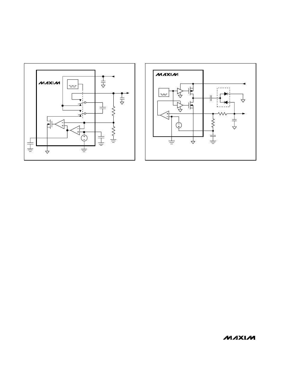
Negative Charge Pump
During the first half-cycle, the P-channel MOSFET turns
on, and flying capacitor C5 charges to V
SUPN
minus a
diode drop (Figure 3). During the second half-cycle,
the P-channel MOSFET turns off, and the N-channel
MOSFET turns on, level shifting C5. This connects C5 in
parallel with the reservoir capacitor, C6. If the voltage
across C6 minus a diode drop is lower than the voltage
across C5, current flows from C5 to C6 until the diode
(D4) turns off. The amount of charge transferred to the
output is controlled by the variable N-channel R
ON
.
Positive Charge Pump
During the first half-cycle, the N-channel MOSFET turns
on and charges the flying capacitor, C3 (Figure 4). This
initial charge is controlled by the variable N-channel
R
ON
. During the second half-cycle, the N-channel
MOSFET turns off, and the P-channel MOSFET turns
on, level shifting C3 by V
SUPP
volts. This connects C3
in parallel with the reservoir capacitor, C4. If the voltage
across C4 plus a diode drop (V
POS
+ V
DIODE
) is small-
er than the level-shifted flying capacitor voltage (V
C3
+
V
SUPP
), charge flows from C3 to C4 until the diode (D2)
turns off.
Frequency Selection and Shutdown
The shutdown pin (SHDN) on the MAX1747 performs a
dual function: it shuts down the device and determines
the oscillator frequency. The SHDN input looks like a
diode to ground and should be driven through a resis-
tor (Figure 5).
Driving SHDN low forces all three MAX1747 converters
into shutdown mode. When disabled, the supply cur-
rent drops to 20µA (max) to maximize battery life, and
OUT is pulled to ground through an internal 10
Ω resis-
tor. For the low-power charge pumps, the output
capacitance and load current determine the rate at
which each output voltage will decay. The device acti-
vates (see Power-up Sequencing) once SHDN is for-
ward biased (minimum of 3µA of current). Do not leave
SHDN floating. For a typical application where shut-
down is used only to set the switching frequency, con-
nect SHDN to the input (V
IN
= 3.3V) with a 120k
Ω
resistor for a 1MHz switching frequency.
The bias current into SHDN, programmed with an exter-
nal resistor, determines the oscillator frequency (see
Typical Operating Characteristics). To select the fre-
quency, calculate the external resistor value, R
FREQ
,
using the following formula:
R
FREQ
= 45.5 (MHz / mA)
✕
(V
ON
– 0.7V) / f
OSC
where R
FREQ
is in k
Ω and f
OSC
is in MHz. Program the
frequency in the 200kHz to 2MHz range. This frequen-
cy range corresponds to SHDN input currents between
3µA to 65µA. Proper operation of the oscillator is not
guaranteed beyond these limits. Forcing SHDN below
400mV disables the device.
Soft-Start
For the MAX1747, soft-start is achieved by controlling
the rise rate of the output voltage, regardless of output
capacitance or output load, and limited only by the out-
put impedance of the regulator (see Startup Waveforms
SUPM
C1
V
SUPM
= V
IN
2.7V TO 4.5V
R1
CX
R2
V
OUT
= [1+ (R1/R2)]
✕
V
REF
V
REF
= 1.25V
GND
V
REF
1.25V
PGND
INTG
C
INTG
REF
FB
CXN
CXP
OUT
OSC
MAX1747
V
OUT
C
OUT
C
REF
gm
Figure 2. Main Charge-Pump Block Diagram
MAX1747
OSC
V
REF
1.25V
GND
PGND
SUPN
DRVN
FBN
REF
R6
C
REF
V
NEG
= -(R5/R6)
✕
V
REF
V
REF
= 1.25V
C6
V
NEG
R5
D3
C5
D4
V
SUPP
= 2.7V TO 13V
Figure 3. Negative Charge-Pump Block Diagram
