Max1747 triple charge-pump tft lcd dc-dc converter, Detailed description, Pin description – Rainbow Electronics MAX1747 User Manual
Page 8
MAX1747
Triple Charge-Pump TFT LCD
DC-DC Converter
8
_______________________________________________________________________________________
Detailed Description
The MAX1747 is an efficient triple-output power supply
for TFT LCD applications. The device contains one
high-power charge pump and two low-power charge
pumps. The MAX1747 charge pumps switch continu-
ously at a constant frequency, so the output noise con-
tains well-defined frequency components, and the
circuit requires much smaller external capacitors for a
given output ripple. The adjustable switching frequency
is set by the current into the shutdown pin (see
Frequency Selection and Shutdown).
The main charge pump uses internal MOSFETs with
low R
ON
to provide high output current. The adjustable
output voltage of the main charge pump can be set up
to 5.5V with external resistors. The dual low-power
charge pumps independently regulate a positive output
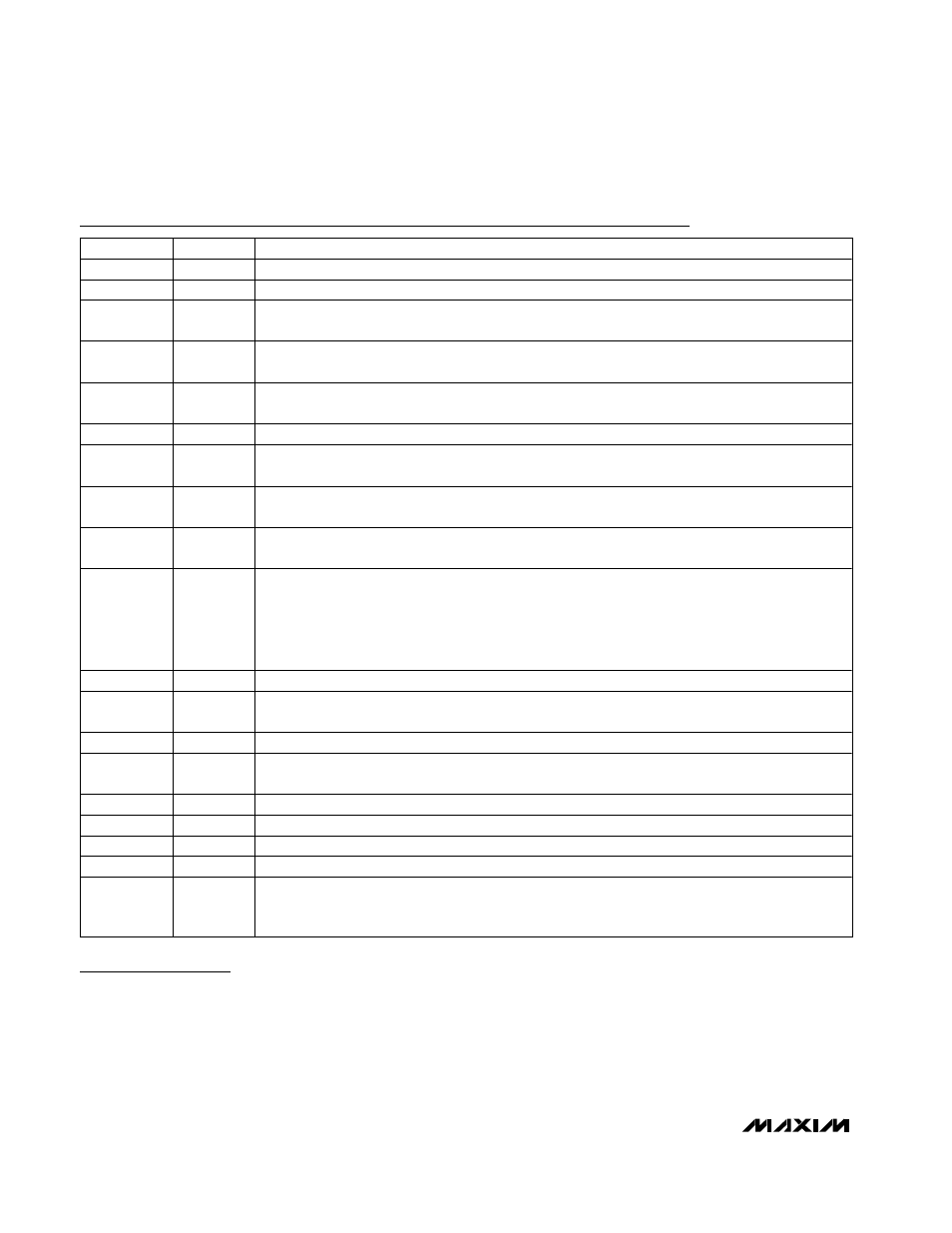
PIN
NAME
FUNCTION
1, 2
TGND
Must be connected to ground.
3
RDY
Active-Low Open-Drain Output. Indicates all outputs are ready. The R
ON
is 125
Ω (typ).
4
FB
Main Charge-Pump Feedback Input. Regulates to 1.25V nominal. Connect to the center of a
feedback resistive divider between the main output (OUT) and analog ground (GND).
5
INTG
Main Charge-Pump Integrator Output. If used, connect 1500pF to analog ground (GND). To disable
the integrator, connect to GND.
6
IN
Supply Input. +2.7V to +4.5V input range. Powers only the logic and reference. Bypass to analog
ground (GND) with a 0.1
µF capacitor as close to the pin as possible.
7
GND
Analog Ground. Connect to power ground (PGND) underneath the IC.
8
REF
Internal Reference Bypass Terminal. Connect a 0.22
µF capacitor from this terminal to analog
ground (GND). External load capability to 50
µA. REF is disabled in shutdown.
9
FBP
Positive Charge-Pump Feedback Input. Regulates to 1.25V nominal. Connect feedback resistive
divider to analog ground (GND).
10
FBN
Negative Charge-Pump Regulator Feedback Input. Regulates to 0V nominal. Connect feedback
resistive divider to the reference (REF).
11
SHDN
Shutdown Input. Drive SHDN through an external resistor. When SHDN is pulled low, the device
turns off and draws only 0.1
µA. OUT is also pulled low through an internal 10Ω resistor in shutdown
mode. When current is sourced into SHDN through R
FREQ
, the device activates, and the SHDN
input current sets the oscillator’s switching frequency:
R
FREQ
(k
Ω) = 45.5 (MHz / mA)
✕
(V
ON
- 0.7V) / f
OSC
(MHz)
12
DRVN
Negative Charge-Pump Driver Output. Output high level is V
SUPN
, and low level is PGND.
13
SUPN
Negative Charge-Pump Driver Supply Voltage. Bypass to power ground (PGND) with a 0.1
µF
capacitor.
14
DRVP
Positive Charge-Pump Driver Output. Output high level is V
SUPP
and low level is PGND.
15
SUPP
Positive Charge-Pump Driver Supply Voltage. Bypass to power ground (PGND) with a 0.1
µF
capacitor.
16
PGND
Power Ground. Connect to analog ground (GND) underneath the IC.
17
CXN
Negative Terminal of the Main Charge-Pump Flying Capacitor
18
SUPM
Main Charge-Pump Supply Voltage Input
19
CXP
Positive Terminal of the Main Charge-Pump Flying Capacitor
20
OUT
Main Charge-Pump Output. Bypass to power ground (PGND) with 10
µF for a 1MHz application
(see Output Capacitor Selection). An internal 10
Ω resistor discharges the output when the device
is shut down.
Pin Description