Max1747 triple charge-pump tft lcd dc-dc converter – Rainbow Electronics MAX1747 User Manual
Page 13

MAX1747
Triple Charge-Pump TFT LCD DC-DC Converter
Maxim cannot assume responsibility for use of any circuitry other than circuitry entirely embodied in a Maxim product. No circuit patent licenses are
implied. Maxim reserves the right to change the circuitry and specifications without notice at any time.
Maxim Integrated Products, 120 San Gabriel Drive, Sunnyvale, CA 94086 408-737-7600 ____________________ 13
© 2000 Maxim Integrated Products
Printed USA
is a registered trademark of Maxim Integrated Products.
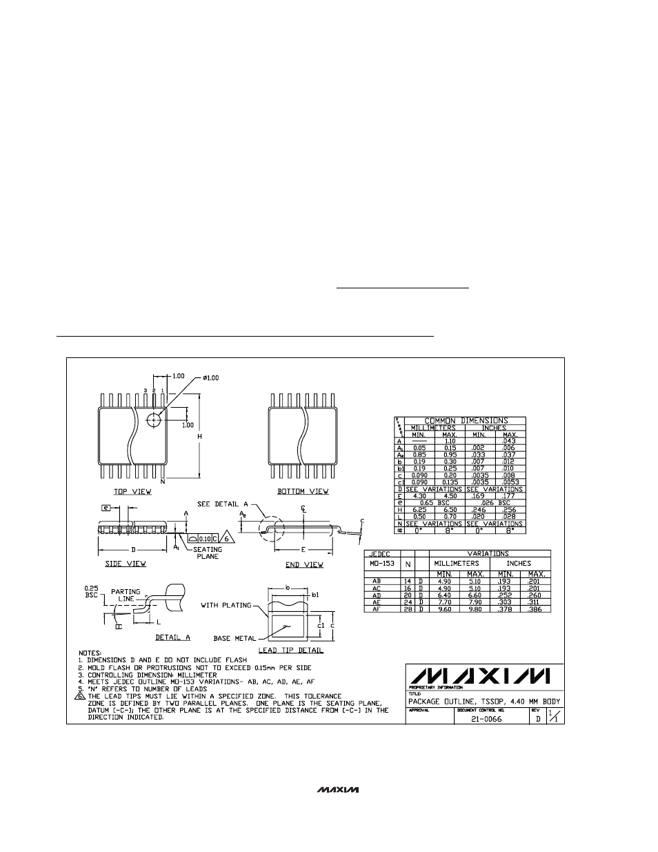
Package Information
PC Board Layout and Grounding
Careful printed circuit layout is important to minimize
ground bounce and noise. First, place the main charge-
pump flying capacitor less than 0.2in (5mm) from the
CXP and CXN pins with wide traces and no vias. Then
place 0.1µF ceramic bypass capacitors near the
charge-pump input pins (SUPP and SUPN) to the
PGND pin. Keep the charge-pump circuitry as close to
the IC as possible, using wide traces and avoiding vias
when possible. Locate all feedback resistive dividers as
close to their respective feedback pins as possible. The
PC board should feature separate analog and power
ground areas connected at only one point under the IC.
To maximize output power and efficiency, and minimize
output power ripple voltage, use extra-wide power
ground traces, and solder the IC’s power ground pin
directly to it. Avoid having sensitive traces near the
switching nodes and high-current lines.
Refer to the MAX1747 evaluation kit for an example of
proper board layout.
Chip Information
TRANSISTOR COUNT: 2534
TSSOP,NO PADS.EPS
