Pin description – Rainbow Electronics MAX1638 User Manual
Page 6
MAX1638
High-Speed Step-Down Controller with
Synchronous Rectification for CPU Power
6
_______________________________________________________________________________________
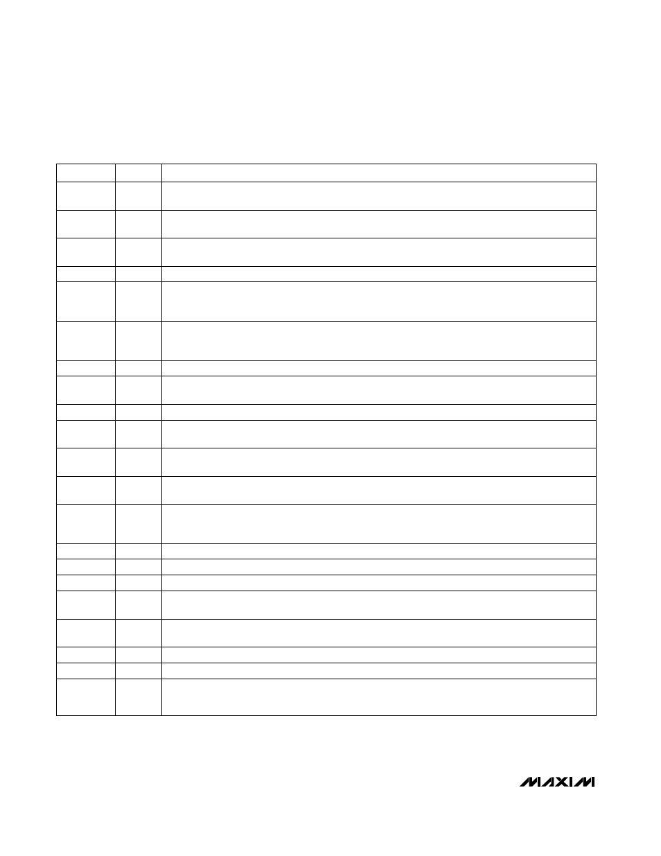
PIN
High-Side Main MOSFET Switch Gate-Drive Output. DH is a floating driver output that swings from LX
to BST, riding on the LX switching-node voltage. See the section
BST High-Side Gate-Driver Supply
and MOSFET Drivers.
DH
24
Switching Node. Connect LX to the high-side MOSFET source and inductor.
LX
23
Power Ground
PGND
22
DL
Low-Side Synchronous Rectifier Gate-Drive Output. DL swings between PGND and V
DD
. See the
section
BST High-Side Gate-Driver Supply and MOSFET Drivers.
21
V
DD
5V Power Input for MOSFET Drivers. Bypass V
DD
to PGND within 0.2 in. (5mm) of the V
DD
pin using a
0.1µF capacitor and 4.7µF capacitor connected in parallel.
20
PDRV
GlitchCatcher P-Channel MOSFET Driver Output. PDRV swings between V
DD
and PGND.
19
NDRV
GlitchCatcher N-Channel MOSFET Driver Output. NDRV swings between V
DD
and PGND.
18
D4, D3
Digital Inputs for Programming the Output Voltage
16, 17
FREQ
Frequency-Select Input. FREQ = V
CC
: 1MHz
FREQ = REF: 600kHz
FREQ = AGND: 300kHz
15
CC2
Slow-Loop Compensation Capacitor Input. Connect a ceramic capacitor from CC2 to AGND. See the
section
Compensating the Feedback Loop.
14
BST
Boost-Capacitor Bypass for High-Side MOSFET Gate Drive. Connect a 0.1µF capacitor and low-leak-
age Schottky diode as a bootstrapped charge-pump circuit to derive a 5V gate drive from V
DD
for DH.
1
NAME
FUNCTION
______________________________________________________________Pin Description
CC1
Fast-Loop Compensation Capacitor Input. Connect a ceramic capacitor and resistor in series from
CC1 to AGND. See the section
Compensating the Feedback Loop.
13
FB
Voltage-Feedback Input. Connect FB to the CPU’s remote voltage-sense point. The voltage at this input
is regulated to a value determined by D0–D4.
12
PWROK
Open-Drain Logic Output. PWROK is high when the voltage on FB is within +8% and -6% of its set-
point.
2
CSL
Current-Sense Amplifier’s Inverting Input. Place the current-sense resistor very close to the controller IC,
and use a Kelvin connection.
3
CSH
Current-Sense Amplifier’s Noninverting Input
4
D2, D1,
D0
Digital Inputs for Programming the Output Voltage. D0–D4 are logic inputs that set the output to a volt-
age between 1.3V and 3.5V (Table 2). D0–D4 are internally pulled up to V
CC
with 5µA current sources.
5, 6, 7
LG
Loop Gain-Control Input. LG is a three-level input that is used to trade off loop gain vs. AC load-regula-
tion and load-transient response. Connect LG to V
CC
, REF, or AGND for 2%, 1%, or 0.5% AC load-reg-
ulation errors, respectively.
8
V
CC
Analog Supply Input, 5V. Use an RC filter network, as shown in Figure 1.
9
REF
Reference Output, 3.5V. Bypass REF to AGND with 0.1µF (min). Sources up to 100µA for external
loads. Force REF below 2V to turn off the controller.
10
AGND
Analog Ground
11