Rainbow Electronics MAX1638 User Manual
Page 2
MAX1638
High-Speed Step-Down Controller with
Synchronous Rectification for CPU Power
2
_______________________________________________________________________________________
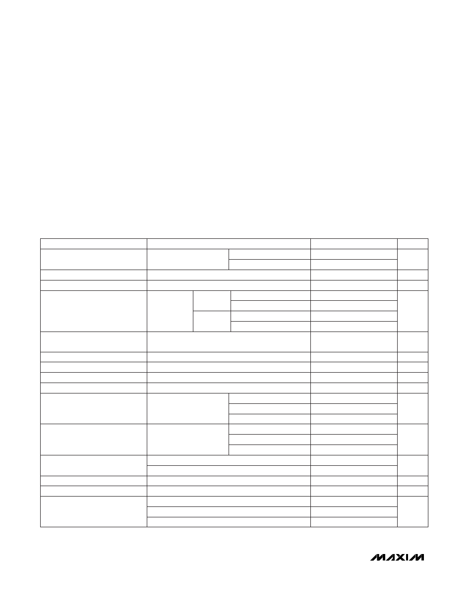
ABSOLUTE MAXIMUM RATINGS
ELECTRICAL CHARACTERISTICS
(V
DD
= V
CC
= D4 = +5V, PGND = AGND = D0–D3 = 0V, FREQ = REF,
T
A
= 0°C to +85°C
, unless otherwise noted.)
Stresses beyond those listed under “Absolute Maximum Ratings” may cause permanent damage to the device. These are stress ratings only, and functional
operation of the device at these or any other conditions beyond those indicated in the operational sections of the specifications is not implied. Exposure to
absolute maximum rating conditions for extended periods may affect device reliability.
V
DD
, V
CC
, PWROK to AGND ......................................-0.3V to 6V
PGND to AGND ..................................................................±0.3V
CSH, CSL to AGND ....................................-0.3V to (V
CC
+ 0.3V)
NDRV, PDRV, DL to PGND.........................-0.3V to (V
DD
+ 0.3V)
REF, CC1, CC2, LG, D0–D4, FREQ,
FB to AGND .............................................-0.3V to (V
CC
+ 0.3V)
BST to PGND ............................................................-0.3V to 12V
BST to LX ....................................................................-0.3V to 6V
DH to LX.............................................(LX - 0.3V) to (BST + 0.3V)
Continuous Power Dissipation (T
A
= +70°C)
QSOP (derate 8.70mW/°C above +70°C) .....................696mW
QSOP
θ
JC
..................................................................40°C/W
SSOP (derate 8.00mW/°C above +70°C) .....................640mW
SSOP
θ
JC
..................................................................45°C/W
Operating Temperature Range ...........................-40°C to +85°C
Storage Temperature Range .............................-65°C to +160°C
Lead Temperature (soldering, 10sec) .............................+300°C
FREQ = AGND
FREQ = REF
V
CC
= V
DD
FREQ = V
CC
PWROK = 5.5V
Over line and load
(Note 1)
I
SINK
= 2mA, V
CC
= 4.5V
Falling FB, 1% hysteresis with respect to V
REF
Rising FB, 1% hysteresis with respect to V
REF
CSH - CSL =
0mV to 80mV
0µA < I
REF
< 100µA
No load
V
CC
= V
DD
= 5.5V, FB forced 200mV above
regulation point, operating or standby mode
V
CC
rising edge, 1% hysteresis
V
REF
= 0V
Rising edge, 1% hysteresis
CONDITIONS
kHz
255
300
345
Switching Frequency
540
600
660
850
1000
1150
µA
1
PWROK Output Current High
V
0.4
PWROK Output Voltage Low
%
6.5
8
9.5
PWROK Trip Level
-7.5
-6
-4.5
%
2
AC Load Regulation
(Note 2)
1
0.5
mA
0.5
4.0
Reference Short-Circuit Current
V
2.7
3.0
Reference Undervoltage Lockout
V
4.5
5.5
Input Voltage Range
%
±1.5
±1
Output Voltage (FB) Accuracy
mV
10
Reference Load Regulation
V
3.465
3.5
3.535
Reference Voltage
mA
0.1
V
DD
Supply Current
V
4.0
4.2
Input Undervoltage Lockout
UNITS
MIN
TYP
MAX
PARAMETER
CSH - CSL =
0mV to 80mV
%
0.2
DC Load Regulation
(Note 2)
0.1
0.05
T
A
= +25°C to +85°C
T
A
= 0°C to +85°C
LG = GND
LG = REF
LG = V
CC
LG = GND
LG = REF
LG = V
CC
2.5
FB overdrive = 200mV
5
FB overdrive = 0V
Operating
mode
V
CC
= V
DD
= 5.5V
mA
3.6
10
V
CC
Supply Current
V
REF
= 0V
Shutdown
mode
0.3
DAC code = 11111