Rainbow Electronics MAX1638 User Manual
Page 15

MAX1638
High-Speed Step-Down Controller with
Synchronous Rectification for CPU Power
______________________________________________________________________________________
15
should be less than 200nC to minimize switching losses
and reduce power dissipation.
I
2
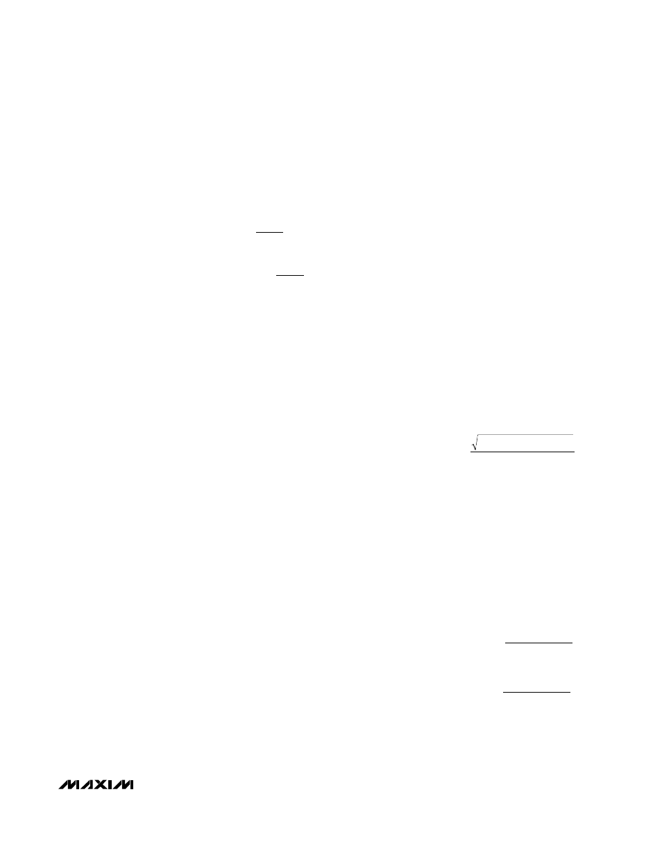
R losses are the greatest heat contributor to MOSFET
power dissipation and are distributed between the
high- and low-side MOSFETs according to duty factor,
as follows:
Gate-charge losses are dissipated in the IC, and do not
heat the MOSFETs. Ensure that both MOSFETs are at a
safe junction temperature by calculating the temperature
rise according to package thermal-resistance specifica-
tions. The high-side MOSFET’s worst-case dissipation
occurs at the maximum output voltage and minimum
input voltage. For the low-side MOSFET, the worst case is
at the maximum input voltage when the output is short-
circuited (consider the duty factor to be 100%).
Calculating IC Power Dissipation
Power dissipation in the IC is dominated by average
gate-charge current into both MOSFETs. Average cur-
rent is approximately:
I
DD
= (Q
G1
+ Q
G2
) x f
OSC
where I
DD
is the drive current, Q
G
is the total gate
charge for each MOSFET, and f
OSC
is the switching
frequency.
Power dissipation of the IC is:
P
D
= I
CC
x V
CC
+ I
DD
x V
DD
where I
CC
is the quiescent supply current of the IC.
Junction temperature for the IC is primarily a function of
the PC board layout, since most of the heat is removed
through the traces connected to the pins and the
ground and power planes. A 24-pin SSOP on a typical
four-layer board with ground and power planes show
equivalent thermal impedance of about 60°C/W.
Junction temperature of the die is approximately:
T
J
= P
D
x
θ
JA
+ T
A
where T
A
is the ambient temperature and
θ
JA
is the
equivalent junction-to-ambient thermal impedance.
Selecting the Rectifier Diode
The rectifier diode D1 is a clamp that catches the nega-
tive inductor swing during the 30ns typical dead time
between turning off the high-side MOSFET and turning on
the low-side MOSFET synchronous rectifier. D1 must be a
Schottky diode, to prevent the MOSFET body diode from
conducting. It is acceptable to omit D1 and let the body
diode clamp the negative inductor swing, but efficiency
will drop about 1%. Use a 1N5819 diode for loads up to
3A, or a 1N5822 for loads up to 10A.
Adding the BST Supply Diode
and Capacitor
A signal diode, such as a 1N4148, works well for D2 in
most applications, although a low-leakage Schottky diode
provides slightly improved efficiency. Do not use large
power diodes, such as the 1N4001 or 1N5817. Exercise
caution in the selection of Schottky diodes, since some
types exhibit high reverse leakage at high operating tem-
peratures. Bypass BST to LX using a 0.1µF capacitor.
Selecting the Input Capacitors
Place a 0.1µF ceramic capacitor and 10µF capacitor
between V
CC
and AGND, as well as between V
DD
and
PGND, within 0.2 in. (5mm) of the V
CC
and V
DD
pins.
Select low-ESR input filter capacitors with a ripple-
current rating exceeding the RMS input ripple current,
connecting several capacitors in parallel if necessary.
RMS input ripple current is determined by the input
voltage and load current, with the worst-possible case
occurring at V
IN
= 2 x V
OUT
:
Choosing the GlitchCatcher MOSFETs
P-channel and N-channel switches and a series resistor
are required for the current-boost circuit (Figure 6).
Current through the MOSFETs and current-limiting
resistors must be sufficient to supply the load current,
with enough extra for prompt output regulation without
excessive overshoot. Design for boost-current values
1.5 times the maximum load current, and choose
MOSFETs and current-limiting resistors such that:
Gate resistors may be required to slow the transition
edges.
R
R
V
V
I
and
R
R
V
I
DSON P MAX
LIMIT
IN
OUT
OUT MAX
DSON N MAX
LIMIT
OUT
OUT MAX
, (
)
(
)
, (
)
(
)
.
.
+
≈
−
+
≈
1 5
1 5
I
I
V
V
V
V
I
I
when V
V
RMS
LOAD MAX
OUT
IN
OUT
IN
RMS
OUT
IN
OUT
(
)
/
(
)
=
−
=
=
2
2
P
low side
I
x R
x
V
V
D
LOAD
DS ON
OUT
IN
(
)
(
)
=
−
2
1
P
high side
I
x R
x
V
V
D
LOAD
DS ON
OUT
IN
(
)
(
)
=
2
