Ac electrical characteristics (max2656) – Rainbow Electronics MAX2656 User Manual
Page 4
MAX2654/MAX2655/MAX2656
1575MHz/1900MHz Variable-IP3
Low-Noise Amplifiers
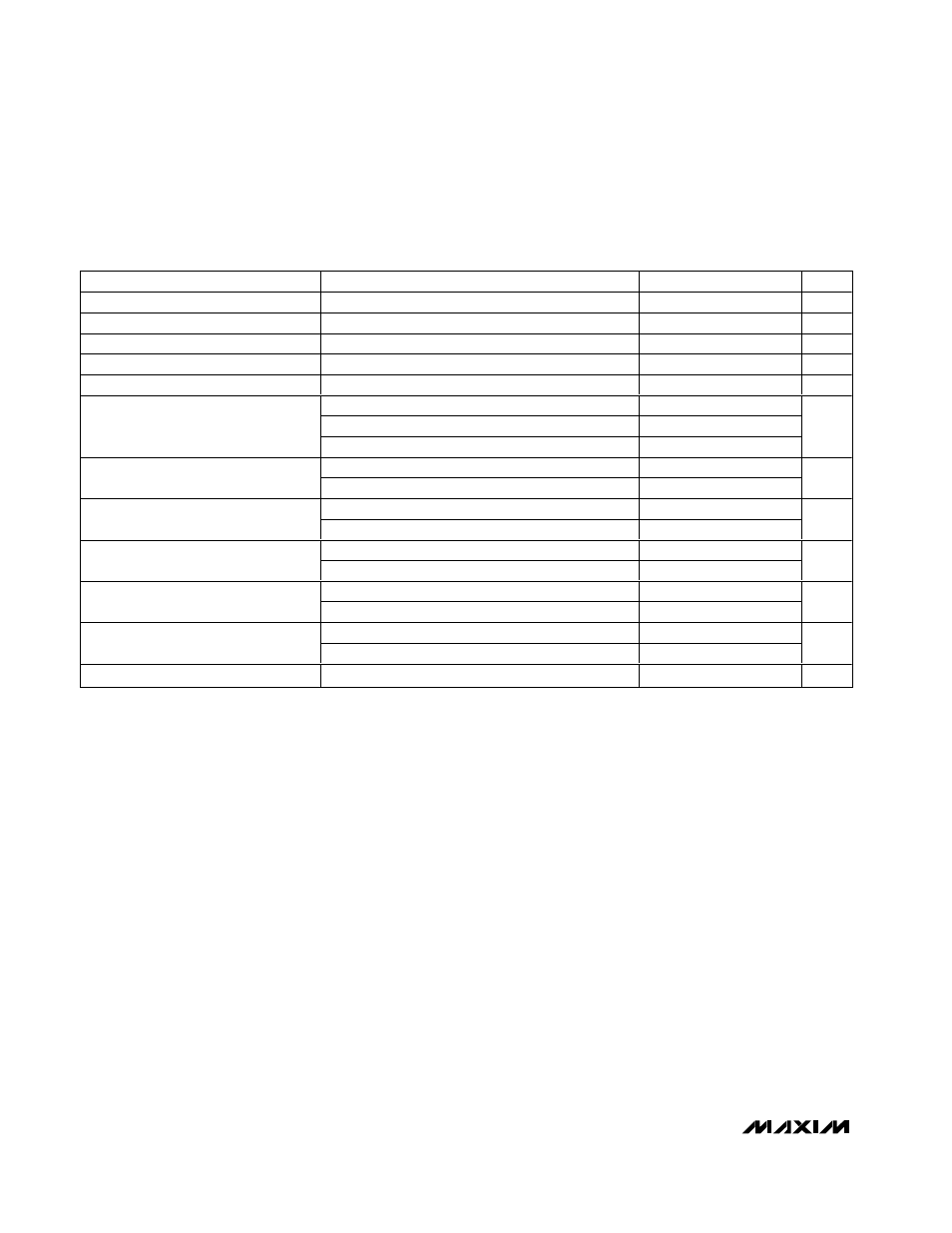
AC ELECTRICAL CHARACTERISTICS (MAX2656)
(MAX2656 Evaluation Kit, V
CC
= +3V, P
IN
= -30dBm, f
IN
= 1960MHz, V
RFOUT
= GND through a 12k
Ω resistor, R
BIAS
= 511
Ω ±1%, T
A
= +25°C. Typical values are at V
CC
= +3V, T
A
= +25°C, unless otherwise noted.) (Note 6)
PARAMETER
CONDITIONS
MIN
TYP
MAX
UNIT
Operating Frequency Range (Note 7)
1800
2000
MHz
Gain, High-Gain Mode
(Note 11)
12
13.5
dB
Gain, Low-Gain Mode
(Note 12)
0.8
dB
Gain Variation Over Temperature
T
A
= -40°C to +85°C
0.3
1.2
dB
Gain Step
12.7
dB
R
BIAS
= 511
Ω ± 1%
1.5
R
BIAS
= 715
Ω ± 1%
-3
Input Third-Order Intercept Point
(Note 13)
Low-gain mode (Note 12)
7.2
dBm
High-gain mode (Note 11)
-7
Input 1dB Compression Point
Low-gain mode (Note 12)
-1.2
dBm
High-gain mode (Note 11)
1.9
2.4
Noise Figure (Note 10)
Low-gain mode (Note 12)
10.8
dB
High-gain mode (Note 11)
14.4
Input Return Loss
Low-gain mode (Note 12)
19.3
dB
High-gain mode (Note 11)
10.7
Output Return Loss
Low-gain mode (Note 12)
7.3
dB
High-gain mode (Note 11)
28
Reverse Isolation
Low-gain mode (Note 12)
25
dB
Gain Step Response Time
3.2
µs
Note 1:
Devices are production tested at T
A
= +25°C. Minimum and maximum values are guaranteed by design and characteriza-
tion over temperature and supply voltages to ±6 sigma.
Note 2:
Minimum DC voltage through a 10k
Ω resistor that sets the MAX2654/MAX2655 to operate in normal mode and MAX2656 in
low-gain mode.
Note 3:
Maximum DC voltage through a 10k
Ω resistor that sets the MAX2654/MAX2655 to operate in shutdown mode and
MAX2656 in high-gain mode.
Note 4:
DC current required when V
RFOUT
is connected to V
CC
through a 10k
Ω resistor.
Note 5:
DC current required when V
RFOUT
is connected to GND through a 10k
Ω resistor.
Note 6:
Guaranteed by design and characterization to ±3 sigma.
Note 7:
The part has been characterized at the specified frequency range. Operation outside of this range is possible, but not
guaranteed.
Note 8:
Production tested at T
A
= +25°C.
Note 9:
Measured with two input tones, f
1
= 1570MHz, f
2
= 1580MHz, both at -30dBm per tone.
Note 10: Excludes PC board losses of 0.2dB for MAX2654/MAX2655 and 0.25dB for MAX2656.
Note 11: High-gain mode is set up by connecting RFOUT to GND through a 12k
Ω resistor.
Note 12: Low-gain mode is set up by connecting RFOUT to V
CC
through a 12k
Ω resistor.
Note 13: Measured with two input tones, f
1
= 1955MHz, f
2
= 1965MHz, both at -30dBm per tone.
4
______________________________________________________________________________________