Detailed description, Pin description, Table 1. r – Rainbow Electronics MAX2656 User Manual
Page 12: Table 2. r
MAX2654/MAX2655/MAX2656
1575MHz/1900MHz Variable-IP3
Low-Noise Amplifiers
12
______________________________________________________________________________________
Detailed Description
The MAX2654/MAX2655/MAX2656 are low-noise ampli-
fiers designed for applications in GPS receivers, satel-
lite and PCS phones. The MAX2655/MAX2656 feature
variable IP3s, adjusted by a single external bias resis-
tor. Another feature of the MAX2654/MAX2655 is a
power shutdown control mode, eliminating the need for
an external supply switch. The MAX2656 features a
high- and low-gain control mode selected by an exter-
nal logic control.
Input and Output Ports
The MAX2654/MAX2655/MAX2656 incorporate on-chip
matching networks to 50
Ω at the output ports, eliminat-
ing the need for external matching components. (For
MAX2655, a shunt inductor is recommended for best
output return loss. Refer to the MAX2655 EV kit
schematic.) The MAX2654/MAX2655/MAX2656 require
simple matching networks at the input ports. The values
of these matching components are recommended in
the Typical Operating Circuit.
Variable IP3
The IP3 of MAX2655 and MAX2656 is adjusted through
an external resistor (R
BIAS
). Tables 1 and 2 summarize
the values of R
BIAS
for different IP3s for MAX2655 and
MAX2656.
Gain-Step Control (MAX2656)
The DC bias voltage at RFOUT of the MAX2656 serves
as a gain-step control input. When the applied DC volt-
age at RFOUT through a 10k
Ω resistor is less than
+0.6V, the device is in high-gain mode. When the
applied DC voltage is greater than +2.0V, the device
gain is attenuated by 13dB. A standard logic output
can be applied as shown in the Typical Operating
Circuit.
Shutdown-Enable (MAX2654/MAX2655)
The DC bias voltage at RFOUT of the MAX2654/
MAX2655 serves as a shutdown enable input. When the
applied DC voltage at RFOUT through a 10k
Ω resistor
is less than +0.6V, the device is in shutdown mode.
When the DC voltage is greater than +2V, the device is
enabled.
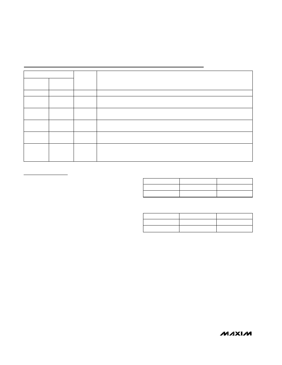
Pin Description
Table 1. R
BIAS
vs. IP3 for MAX2655
R
BIAS
(
Ω)
IP3 (dBm)
I
CC
(mA)
698
2.2
5.8
357
3.8
10.1
Table 2. R
BIAS
vs. IP3 for MAX2656
R
BIAS
(
Ω)
IP3 (dBm)
I
CC
(mA)
715
-3
8.5
511
1.5
11.5
PIN
MAX2654
MAX2655/
MAX2656
NAME
DESCRIPTION
1
–––
GND
G r ound . C onnect to the P C b oar d g r ound p l ane thr oug h a 0.017i n x 0.035i n l i ne.
2, 5
2, 5
GND
Ground. Connect to the P C b oar d ground plane with as low an inductance path as
possible.
–––
1
BIAS
Bias Control. Connect a resistor R
BIAS
from BIAS to GND. R
BIAS
sets IP3 and
supply current.
3
3
RFIN
Amplifier Input. Requires a DC-blocking capacitor and external matching components.
4
4
V
CC
Supply Voltage. Bypass to ground with an appropriate capacitor as close to the IC as
possible. Refer to MAX2654/MAX2655/MAX2656 EV kits for capacitor values.
6
6
RFOUT
RF Output. Incorporates an internal DC-blocking capacitor. RFOUT is internally
matched to 50
Ω. DC bias on this pin selects gain mode (MAX2656) or shutdown mode
(MAX2654/MAX2655) (see Applications Information).