Step-up dc-dc controller, Detailed description – Rainbow Electronics MAX1771 User Manual
Page 7
MAX1771
12V or Adjustable, High-Efficiency,
Low I
Q
, Step-Up DC-DC Controller
_______________________________________________________________________________________
7
Detailed Description
The MAX1771 is a BiCMOS, step-up, switch-mode
power-supply controller that provides a preset 12V out-
put, in addition to adjustable-output operation. Its
unique control scheme combines the advantages of
pulse-frequency modulation (low supply current) and
pulse-width modulation (high efficiency with heavy
loads), providing high efficiency over a wide output
current range, as well as increased output current
capability over previous PFM devices. In addition, the
external sense resistor and power transistor allow the
user to tailor the output current capability for each appli-
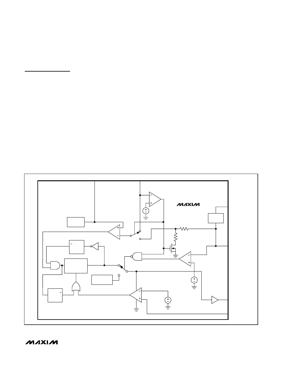
cation. Figure 1 shows the MAX1771 functional diagram.
The MAX1771 offers three main improvements over
prior pulse-skipping control solutions: 1) the converter
operates with miniature (5mm height and less than
9mm diameter) surface-mount inductors due to its
300kHz switching frequency; 2) the current-limited PFM
control scheme allows 90% efficiencies over a wide
range of load currents; and 3) the maximum supply
current is only 110µA.
The device has a shutdown mode that reduces the
supply current to 5µA max.
Bootstrapped/Non-Bootstrapped Modes
Figure 2 shows the standard application circuits for
bootstrapped and non-bootstrapped modes. In boot-
strapped mode, the IC is powered from the output
(V
OUT
, which is connected to V+) and the input voltage
range is 2V to V
OUT
. The voltage applied to the gate of
the external power transistor is switched from V
OUT
to
ground, providing more switch gate drive and thus
reducing the transistor’s on-resistance.
In non-bootstrapped mode, the IC is powered from the
input voltage (V+) and operates with minimum supply
current. In this mode, FB is the output voltage sense
point. Since the voltage swing applied to the gate of the
external power transistor is reduced (the gate swings
from V+ to ground), the power transistor’s on-resistance
1.5V
REFERENCE
Q
TRIG
Q
S
F/F
R
Q
TRIG
LOW-VOLTAGE
OSCILLATOR
2.5V
0.1V
MAX ON-TIME
ONE-SHOT
MIN OFF-TIME
ONE-SHOT
CURRENT-SENSE
AMPLIFIER
DUAL-MODE
COMPARATOR
FB
REF
50mV
ERROR
COMPARATOR
SHDN
V+
EXT
CS
BIAS
CIRCUITRY
N
MAX1771
2.3
µs
16
µs
Figure 1. Functional Diagram